
AT40K20LV-3DQC
| Part Description |
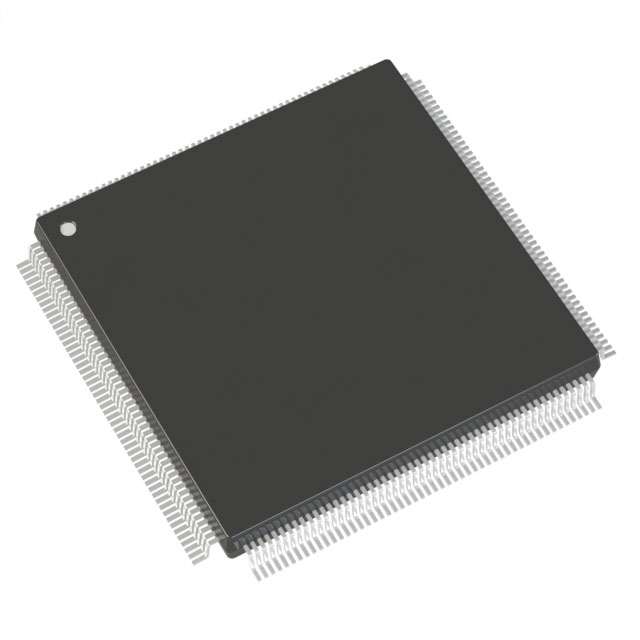
AT40K/KLV Field Programmable Gate Array (FPGA) IC 161 8192 1024 208-BFQFP |
|---|---|
| Quantity | 46 Available (as of October 7, 2026) |

| Product Category | Field Programmable Gate Array (FPGA) |
|---|---|
| Manufacturer | Microchip Technology |
| Manufacturing Status | Obsolete |
| Manufacturer Standard Lead Time | Contact Us |
| Datasheet |
Specifications & Environmental
| Device Package | 208-PQFP (28x28) | Grade | Commercial | Operating Temperature | 0°C – 70°C | ||
|---|---|---|---|---|---|---|---|
| Package / Case | 208-BFQFP | Number of I/O | 161 | Voltage | 3 V - 3.6 V | ||
| Mounting Method | Surface Mount | RoHS Compliance | RoHS non-compliant | REACH Compliance | REACH Unaffected | ||
| Moisture Sensitivity Level | 3 (168 Hours) | Number of LABs/CLBs | 1024 | Number of Logic Elements/Cells | 1024 | ||
| Number of Gates | 30000 | ECCN | 3A991D | HTS Code | 8542.39.0001 | ||
| Qualification | N/A | Total RAM Bits | 8192 |
Overview of AT40K20LV-3DQC – Field Programmable Gate Array (FPGA), 1,024 Logic Elements
The AT40K20LV-3DQC is an SRAM-based FPGA from Microchip Technology in the AT40K/AT40KLV family, offering 1,024 logic elements and approximately 30,000 usable gates. It combines distributed, fast embedded SRAM with a reconfigurable logic fabric and a 208-pin surface-mount package for compact, mid-density designs.
Designed for high-performance logic acceleration and DSP-style co-processing tasks, this device suits commercial embedded systems that require on-chip RAM, flexible I/O counts, and system-level reconfigurability.
Key Features
- Logic Capacity 1,024 logic elements (1,024 registers) and approximately 30,000 gates provide mid-range density for control, signal processing, and glue-logic functions.
- Embedded Memory (FreeRAM) Approximately 8,192 bits of distributed on-chip RAM with 10 ns access time; supports flexible single/dual-port and synchronous/asynchronous RAM configurations for FIFOs, scratch pads and buffering.
- High-Speed Operation System speeds to 100 MHz and array multipliers rated for >50 MHz (series characteristic) enable accelerated arithmetic and DSP functions.
- Global Clocking Eight global clock networks with low-skew distribution, programmable edge transitions and distributed clock shutdown for power management and timing control.
- I/O and Package 161 I/O pins in a 208-BFQFP surface-mount package (supplier package: 208-PQFP, 28×28). I/Os in the series support PCI-compliant signaling characteristics and 3 V/5 V capability (series detail).
- Power and Environmental Nominal voltage supply 3.0 V to 3.6 V; commercial operating temperature range 0 °C to 70 °C. RoHS compliant and surface-mount for automated assembly.
- Reconfigurability and System Integration Cache Logic dynamic partial/full re-configurability (series feature), internal tri-state capability in each cell, and pin-compatible package options to simplify migration and board-level substitution.
- Industry Design Tool Support Series provides integration with industry-standard design and synthesis tools, enabling timing-driven placement, routing and reuse of automatic component generators.
Typical Applications
- DSP and Co-processor Acceleration Used as a coprocessor to implement computation-intensive arithmetic like FIR filters, FFTs and vector multipliers to offload processors and speed signal processing tasks.
- Video and Multimedia Processing Implements accelerators for video compression/decompression, DCT/IDCT, and other multimedia functions using the device’s embedded RAM and array multiplier features.
- Encryption & Security Engines Deploys custom encryption, hashing and convolution functions where reconfigurable logic and on-chip memory enable algorithm updates and optimization.
- Custom Control & Glue Logic Mid-density logic for interface bridging, protocol adaptation, and board-level control where compact packaging and abundant I/O are required.
Unique Advantages
- Flexible On-chip Memory: The device’s distributed 10 ns FreeRAM lets you implement multiple independent RAM functions without consuming separate logic resources.
- Reconfigurable In-System Capability: Series Cache Logic supports full or partial reconfiguration in-system, enabling adaptive designs and fast updates of algorithm coefficients.
- Balanced Performance and Density: With 1,024 logic elements and ~8,192 bits of RAM, the device provides a mid-range integration point for DSP and control tasks without excessive board area.
- Deterministic Clocking: Eight global clocks and low-skew distribution simplify multi-clock designs and timing management across the fabric.
- Package and Assembly Friendly: Surface-mount 208-pin BFQFP/PQFP package supports automated assembly and a compact board footprint for commercial applications.
- Toolchain Interoperability: Integration with industry-standard synthesis and simulation tools streamlines design entry, verification and migration across projects.
Why Choose AT40K20LV-3DQC?
The AT40K20LV-3DQC positions itself as a practical, mid-density FPGA solution for commercial embedded systems that need a mix of reconfigurable logic, on-chip RAM and deterministic clocking. Its combination of roughly 1,024 logic elements, 8,192 bits of embedded RAM, and multiple global clocks makes it well suited to DSP acceleration, media processing and custom interface logic.
Supported by the AT40K/AT40KLV series architecture and industry-standard design flows, this device offers scalable design options and in-system reconfiguration capabilities that help reduce BOM complexity and accelerate development cycles for commercial applications.
Request a quote or submit a pricing inquiry today to evaluate AT40K20LV-3DQC for your next design.
























Date Founded: 1989
Headquarters: Chandler, Arizona, USA
Employees: 22,000+
Revenue: $8.349 Billion
Certifications and Memberships: ISO9001:2015, IATF16949:2016, AS 9100D




