
M2GL005-VF400
| Part Description |
IGLOO2 Field Programmable Gate Array (FPGA) IC 169 719872 6060 400-LFBGA |
|---|---|
| Quantity | 741 Available (as of June 14, 2026) |

| Product Category | Field Programmable Gate Array (FPGA) |
|---|---|
| Manufacturer | Microchip Technology |
| Manufacturing Status | Active |
| Manufacturer Standard Lead Time | 10 Weeks |
| Datasheet |
Specifications & Environmental
| Device Package | 400-VFBGA (17x17) | Grade | Commercial | Operating Temperature | 0°C – 85°C | ||
|---|---|---|---|---|---|---|---|
| Package / Case | 400-LFBGA | Number of I/O | 169 | Voltage | 1.14 V - 2.625 V | ||
| Mounting Method | Surface Mount | RoHS Compliance | RoHS non-compliant | REACH Compliance | REACH Unaffected | ||
| Moisture Sensitivity Level | 3 (168 Hours) | Number of LABs/CLBs | 6060 | Number of Logic Elements/Cells | 6060 | ||
| Number of Gates | N/A | ECCN | EAR99 | HTS Code | 8542.39.0001 | ||
| Qualification | N/A | Total RAM Bits | 719872 |
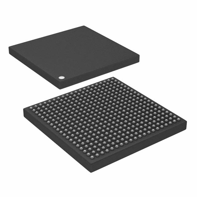
Overview of M2GL005-VF400 – IGLOO2 FPGA, 6060 logic elements, 169 I/Os, 400-LFBGA
The M2GL005-VF400 is a commercial-grade IGLOO2 field programmable gate array (FPGA) from Microchip Technology. It uses IGLOO2's fourth-generation flash-based FPGA fabric and on-chip memory to deliver a reconfigurable logic solution suited to embedded and communications-oriented designs.
This device targets applications that require moderate logic density with extensive I/O and embedded memory, delivered in a compact 400-ball LFBGA package. Key value comes from its flash-based architecture, multi-standard I/O support, and integrated family-level capabilities for high-speed interfaces and security.
Key Features
- Fabric and Architecture IGLOO2 fourth-generation flash-based FPGA fabric with 4-input LUT architecture and carry chains, designed to support reconfigurable logic implementations.
- Logic Density 6060 logic elements for implementing control, glue logic, and moderate-sized programmable functions.
- Embedded Memory Total on-chip RAM of 719,872 bits (approximately 0.72 Mbits) for data buffering and state storage; IGLOO2 family includes additional embedded SRAM and nonvolatile memory options at the family level.
- I/O and Signaling 169 user I/Os with multi-standard support per the IGLOO2 family, enabling a broad range of single-ended and differential interfaces and DDR I/O standards.
- High-Speed Interface Capabilities (family-level) IGLOO2 family-level features include support for high-speed SERDES lanes, PCI Express endpoints, and XAUI/XGMII interfaces when implemented in a design.
- Security Features (family-level) IGLOO2 family includes design security features such as encrypted bitstream loading, device certificates, anti-tamper and zeroization options; premium family devices provide additional cryptographic services and PUF support.
- Power and Supply Wide operating supply range from 1.14 V to 2.625 V to accommodate varying core and I/O rail configurations.
- Package and Mounting 400-LFBGA package, supplier device package 400-VFBGA (17×17 mm); surface-mount mounting for compact board-level integration.
- Commercial Temperature Grade Rated for operating temperatures from 0 °C to 85 °C and RoHS compliant.
Typical Applications
- High-speed communications modules Implement protocol bridging, SERDES-based PHY functions, and packet processing leveraging IGLOO2 family high-speed interface capabilities.
- Embedded control and glue logic Replace multiple discrete components with programmable logic for control, sequencing, and peripheral interfacing using 6060 logic elements and 169 I/Os.
- Memory interface and buffering Use the device's embedded RAM (approximately 0.72 Mbits) for frame buffering, packet queues, and temporary data storage in systems with external DDR memory controllers at the family level.
- DSP and signal-processing helpers Offload math and fixed-function processing to fabric and family-level DSP resources for applications requiring arithmetic acceleration.
Unique Advantages
- Flash-based FPGA fabric: Nonvolatile IGLOO2 architecture enables retained configuration without external configuration memory.
- Balanced logic and memory: 6060 logic elements paired with approximately 0.72 Mbits of on-chip RAM provide a compact platform for control and data buffering tasks.
- Flexible I/O support: 169 user I/Os and multi-standard signaling options support diverse single-ended and differential interface needs on a single device.
- Compact, manufacturable package: 400-LFBGA (supplier 400-VFBGA, 17×17 mm) surface-mount package enables dense board integration while maintaining a high pin count.
- Wide supply range: 1.14 V to 2.625 V supply flexibility helps accommodate different core and I/O voltage architectures.
- Security and system assurance (family features): IGLOO2 family security options such as encrypted bitstreams and device certificates help protect intellectual property and enable trusted deployment models.
Why Choose M2GL005-VF400?
The M2GL005-VF400 combines IGLOO2's flash-based FPGA fabric with 6060 logic elements, approximately 0.72 Mbits of on-chip RAM, and 169 I/Os in a 400-ball LFBGA package. It is well suited for commercial embedded designs that need reconfigurable logic, significant I/O density, and on-chip memory in a compact surface-mount form factor.
This device is appropriate for designs that require moderate programmable logic capacity with multi-standard I/O flexibility and family-level capabilities for high-speed interfaces and security. Its commercial temperature rating and RoHS compliance make it suitable for mainstream electronics and communications applications.
Request a quote or submit a request for pricing and availability for the M2GL005-VF400 to evaluate fit for your next design.


Date Founded: 1989
Headquarters: Chandler, Arizona, USA
Employees: 22,000+
Revenue: $8.349 Billion
Certifications and Memberships: ISO9001:2015, IATF16949:2016, AS 9100D


