
M2GL010-1VF400I
| Part Description |
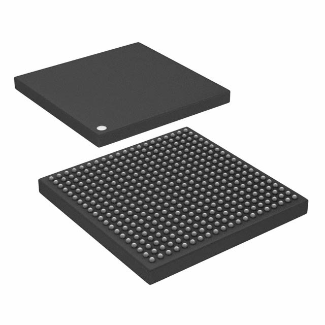
IGLOO2 Field Programmable Gate Array (FPGA) IC 195 933888 12084 400-LFBGA |
|---|---|
| Quantity | 1,965 Available (as of June 15, 2026) |
| Product Category | Field Programmable Gate Array (FPGA) |
|---|---|
| Manufacturer | Microchip Technology |
| Manufacturing Status | Active |
| Manufacturer Standard Lead Time | 10 Weeks |
| Datasheet |
Specifications & Environmental
| Device Package | 400-VFBGA (17x17) | Grade | Industrial | Operating Temperature | -40°C – 100°C | ||
|---|---|---|---|---|---|---|---|
| Package / Case | 400-LFBGA | Number of I/O | 195 | Voltage | 1.14 V - 2.625 V | ||
| Mounting Method | Surface Mount | RoHS Compliance | RoHS non-compliant | REACH Compliance | REACH Unaffected | ||
| Moisture Sensitivity Level | 3 (168 Hours) | Number of LABs/CLBs | 12084 | Number of Logic Elements/Cells | 12084 | ||
| Number of Gates | N/A | ECCN | 3A991D | HTS Code | 8542.39.0001 | ||
| Qualification | N/A | Total RAM Bits | 933888 |
Overview of M2GL010-1VF400I – IGLOO2 FPGA, 400-LFBGA
The M2GL010-1VF400I is an IGLOO2 family field programmable gate array integrating fourth-generation flash-based FPGA fabric with high-performance communications and memory interfaces. It targets industrial applications that require a balance of programmable logic, embedded memory, flexible I/O, and security features.
Key device attributes include 12,084 logic elements, approximately 0.93 Mbits of on-chip RAM, 195 user I/Os, a 400-LFBGA package, and an industrial operating range. The device supports a broad supply voltage window and offers built-in design security capabilities.
Key Features
- Core FPGA Fabric Fourth-generation flash-based fabric with 4-input LUT architecture and carry chains for efficient logic implementation and improved performance.
- Logic Capacity 12,084 logic elements to implement mid-density programmable designs.
- Embedded Memory Approximately 0.93 Mbits of on-chip RAM, with the IGLOO2 family offering multiple embedded memory options to support data buffering and storage.
- DSP and Mathblocks Family-level support for high-performance DSP resources, including mathblocks for signed and unsigned multiplications and accumulation (series-level capability).
- High‑Speed Serial Interfaces IGLOO2 family supports SERDES lanes, XAUI/XGMII extension and PCI Express endpoint controller options for implementing high-speed serial links (family-level features).
- High‑Speed Memory Interfaces Family-level support for DDRx memory controllers (LPDDR/DDR2/DDR3) enabling high-throughput external memory connectivity.
- I/O and Voltage Flexibility 195 user I/Os with multi-standard I/O support; device supply range 1.14 V to 2.625 V and a documented 1.2 V core voltage (series specification).
- Package and Mounting 400-LFBGA surface-mount package; supplier package specified as 400-VFBGA (17 × 17 mm footprint).
- Industrial Temperature and Compliance Rated for operation from −40 °C to 100 °C and RoHS compliant.
- Design Security Features Family-level design security includes encrypted user key and bitstream loading, device certificate for supply-chain assurance, anti-tamper capabilities, and zeroization; additional data-security features are available on premium devices.
Typical Applications
- Networking & Communications Leverage SERDES lanes and PCI Express endpoint capability to implement high-speed links and bridge interfaces in networking equipment.
- High‑Speed Memory Interfaces Use DDRx memory controllers and the on-chip buffering to manage high-throughput memory access in storage and buffering applications.
- Signal Processing Deploy mathblocks and embedded memory for DSP tasks such as filtering, aggregation, and arithmetic-heavy processing in embedded systems.
- Industrial Control & Instrumentation Industrial temperature rating, robust I/O options, and programmable logic make the device suitable for control, monitoring, and I/O aggregation in industrial environments.
Unique Advantages
- Integrated Programmable Logic: 12,084 logic elements provide a compact, programmable platform to consolidate logic functions and reduce external component count.
- On‑Chip Memory: Approximately 0.93 Mbits of embedded RAM supports local data buffering and reduces dependence on external memory for many designs.
- Flexible I/O & Voltage Support: 195 user I/Os and a wide supply voltage range enable mixed-signal interfacing and adaptable board-level designs.
- Industrial Reliability: −40 °C to 100 °C operating range and surface-mount 400-LFBGA packaging support deployment in industrial temperature environments.
- Security-Ready Design: Built-in design security features (encrypted bitstream, device certificate, anti-tamper, zeroization) support secure provisioning and supply-chain assurance.
- Family-Level High-Speed Interfaces: IGLOO2 family support for SERDES, PCIe, and DDRx controllers enables scalable implementation of high-bandwidth system functions.
Why Choose M2GL010-1VF400I?
The M2GL010-1VF400I delivers a well-rounded mid-density FPGA solution combining programmable logic, embedded memory, extensive I/O, and family-level high-speed interfaces. Its industrial temperature rating and surface-mount 400-LFBGA package make it suitable for ruggedized and space-constrained applications.
This device is appropriate for engineers designing communication links, memory-intensive subsystems, DSP-enabled embedded platforms, and industrial control systems that benefit from integrated security features and flexible I/O and power options.
Request a quote or submit an inquiry to receive pricing, availability, and support information for the M2GL010-1VF400I.


Date Founded: 1989
Headquarters: Chandler, Arizona, USA
Employees: 22,000+
Revenue: $8.349 Billion
Certifications and Memberships: ISO9001:2015, IATF16949:2016, AS 9100D


