
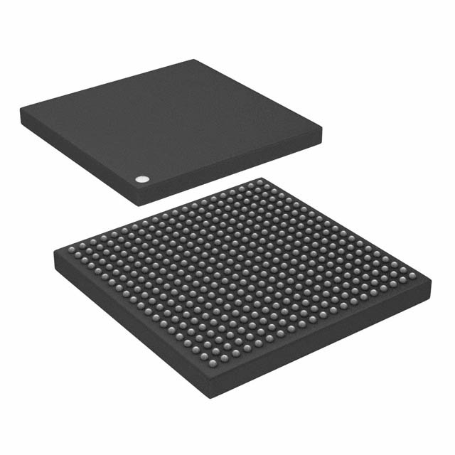
M2GL010-1VFG400
| Part Description |
IGLOO2 Field Programmable Gate Array (FPGA) IC 195 933888 12084 400-LFBGA |
|---|---|
| Quantity | 1,573 Available (as of June 15, 2026) |

| Product Category | Field Programmable Gate Array (FPGA) |
|---|---|
| Manufacturer | Microchip Technology |
| Manufacturing Status | Active |
| Manufacturer Standard Lead Time | 10 Weeks |
| Datasheet |
Specifications & Environmental
| Device Package | 400-VFBGA (17x17) | Grade | Commercial | Operating Temperature | 0°C – 85°C | ||
|---|---|---|---|---|---|---|---|
| Package / Case | 400-LFBGA | Number of I/O | 195 | Voltage | 1.14 V - 2.625 V | ||
| Mounting Method | Surface Mount | RoHS Compliance | ROHS3 Compliant | REACH Compliance | REACH Unaffected | ||
| Moisture Sensitivity Level | 3 (168 Hours) | Number of LABs/CLBs | 12084 | Number of Logic Elements/Cells | 12084 | ||
| Number of Gates | N/A | ECCN | 3A991D | HTS Code | 8542.39.0001 | ||
| Qualification | N/A | Total RAM Bits | 933888 |
Overview of M2GL010-1VFG400 – IGLOO2 Field Programmable Gate Array (FPGA) IC 195 933888 12084 400-LFBGA
The M2GL010-1VFG400 is an IGLOO2 flash-based FPGA from Microchip Technology that combines programmable logic fabric with high-performance communications and memory interfaces. Based on the IGLOO2 architecture, it targets applications that require moderate logic density, embedded memory, DSP capabilities and a range of high-speed serial and DDR memory interfaces.
This device delivers 12,084 logic elements, approximately 0.93 Mbits of embedded memory (933,888 bits), and up to 16 SERDES lanes and DDR memory controller support as described in the IGLOO2 family specification, making it suitable for designs emphasizing low power, integrated memory subsystems and secure operation.
Key Features
- Core Logic 12,084 logic elements providing the programmable fabric for custom logic and control implementations.
- Embedded Memory Approximately 0.93 Mbits of on-chip RAM (933,888 bits) for buffer and state storage.
- DSP and Math IGLOO2 family mathblock support for hardware multiplication and accumulation suitable for signal processing tasks (family-level capability).
- High-Speed Serial Interfaces Family-level support for up to 16 SERDES lanes with native SERDES, XGXS/XAUI and PCIe endpoint options for high-bandwidth data paths.
- High-Speed Memory Interfaces Support for DDRx memory controllers (family-level) including DDR2/DDR3/LPDDR with up to 333 MHz clock rate and multiple DRAM bus width modes.
- I/O and Voltage Flexibility 195 user I/Os with multi-standard I/O options across common voltage domains; device supply range 1.14 V to 2.625 V.
- Clocking Resources Multiple embedded oscillators and up to 8 Clock Conditioning Circuits (CCCs) with integrated PLLs (family-level features) for flexible clock generation and distribution.
- Security Features IGLOO2 family security capabilities including encrypted key and bitstream loading, supply-chain device certificate, anti-tamper and zeroization features; data security options such as AES-256 and SHA-256 available on premium family devices.
- Package and Mounting 400-LFBGA package; supplier device package listed as 400-VFBGA (17×17) and intended for surface-mount assembly.
- Operating Conditions Commercial grade operation with specified operating temperature range 0 °C to 85 °C and RoHS compliance.
Typical Applications
- High-Speed Communications Implement SERDES-based links, PCIe endpoints or XAUI/XGMII interfaces using the IGLOO2 family’s high-speed serial capabilities for network and communications equipment.
- Memory Subsystem and Controllers DDR2/DDR3 and LPDDR interface support allows use as a bridge or controller in systems requiring high-performance external memory access.
- DSP and Signal Processing On-chip mathblock and embedded RAM resources support hardware-accelerated multiplication and accumulation for signal conditioning and real-time processing tasks.
- Secure Embedded Control Encrypted bitstream and anti-tamper features make the device suitable for applications where IP protection and secure configuration are required.
Unique Advantages
- Integrated Memory and Logic: Combines 12,084 logic elements with approximately 0.93 Mbits of embedded RAM, reducing external memory dependency for many control and buffering tasks.
- Flexible I/O and Low-Voltage Operation: 195 I/Os and a broad supply range (1.14 V to 2.625 V) accommodate diverse interfacing requirements and design topologies.
- High-Speed Connectivity Options: Family-level SERDES, PCIe and XAUI/XGMII support enable direct implementation of high-bandwidth serial links without extensive external logic.
- Security and Supply-Chain Assurance: Encrypted key/bitstream loading, device certificates and anti-tamper features help protect IP and support secure deployment models.
- Commercial-Grade Temperature Range: Specified operation from 0 °C to 85 °C for standard commercial applications.
- RoHS Compliant: Meets RoHS requirements for lead-free manufacturing and compliance-driven designs.
Why Choose M2GL010-1VFG400?
The M2GL010-1VFG400 leverages the IGLOO2 family architecture to provide a balanced combination of programmable logic, embedded memory and high-speed interfaces in a 400-LFBGA package. Its feature set supports designs that require moderate logic density, on-chip RAM, secure configuration and flexible I/O in commercial-temperature applications.
This device is well suited to designers who need an FPGA with integrated memory and serial/memory interface capabilities while keeping power and component count down. Backed by Microchip Technology’s IGLOO2 family-level capabilities, it offers a path for scalable designs that require secure configuration and high-speed connectivity.
Request a quote or submit an inquiry to get pricing, availability and additional technical assistance for the M2GL010-1VFG400.


Date Founded: 1989
Headquarters: Chandler, Arizona, USA
Employees: 22,000+
Revenue: $8.349 Billion
Certifications and Memberships: ISO9001:2015, IATF16949:2016, AS 9100D


