
M2GL010T-1VF400
| Part Description |
IGLOO2 Field Programmable Gate Array (FPGA) IC 195 933888 12084 400-LFBGA |
|---|---|
| Quantity | 430 Available (as of June 10, 2026) |

| Product Category | Field Programmable Gate Array (FPGA) |
|---|---|
| Manufacturer | Microchip Technology |
| Manufacturing Status | Active |
| Manufacturer Standard Lead Time | 10 Weeks |
| Datasheet |
Specifications & Environmental
| Device Package | 400-VFBGA (17x17) | Grade | Commercial | Operating Temperature | 0°C – 85°C | ||
|---|---|---|---|---|---|---|---|
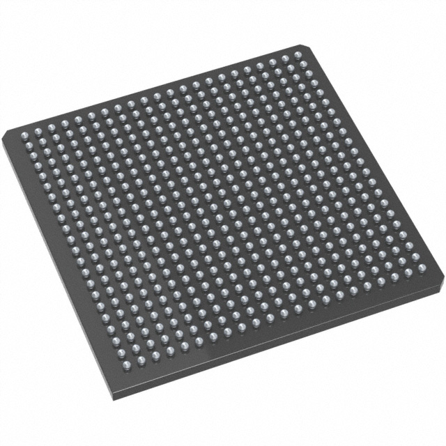
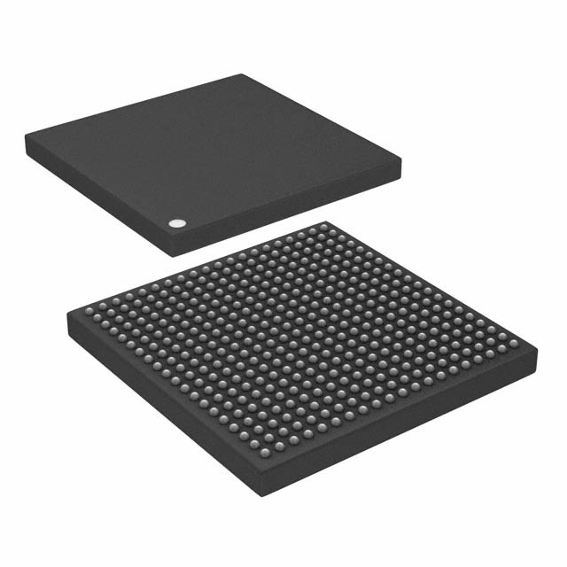
| Package / Case | 400-LFBGA | Number of I/O | 195 | Voltage | 1.14 V - 2.625 V | ||
| Mounting Method | Surface Mount | RoHS Compliance | RoHS non-compliant | REACH Compliance | REACH Unaffected | ||
| Moisture Sensitivity Level | 3 (168 Hours) | Number of LABs/CLBs | 12084 | Number of Logic Elements/Cells | 12084 | ||
| Number of Gates | N/A | ECCN | 3A991D | HTS Code | 8542.39.0001 | ||
| Qualification | N/A | Total RAM Bits | 933888 |
Overview of M2GL010T-1VF400 – IGLOO2 FPGA, 400‑LFBGA
The M2GL010T-1VF400 is an IGLOO2 family flash-based Field Programmable Gate Array (FPGA) from Microchip Technology. It combines a 4‑input LUT fabric with embedded memory and flexible I/O in a 400‑ball LFBGA/VFBGA package for commercial embedded and communications designs.
With 12,084 logic elements, approximately 0.94 Mbits of on-chip RAM (933,888 total RAM bits), and 195 user I/Os, this device targets applications requiring moderate logic capacity, embedded memory, and a broad set of interface and system resources while operating from a 1.14 V to 2.625 V supply and a 0 °C to 85 °C commercial temperature range.
Key Features
- Logic Capacity — 12,084 logic elements (cells) implemented in IGLOO2 4‑input LUT fabric with carry chains for efficient arithmetic and control logic.
- Embedded Memory — 933,888 total RAM bits (approximately 0.94 Mbits) of on-chip memory for buffering and local data storage; IGLOO2 family architecture also documents 64 KB eSRAM and up to 512 KB eNVM.
- DSP and Math Resources — IGLOO2 family supports mathblocks for DSP tasks, enabling signed/unsigned multiplication and accumulation suitable for signal-processing pipelines.
- High‑Speed Interfaces (Family Capabilities) — The IGLOO2 family provides high‑performance serial interfaces including native SERDES, XAUI/XGXS and PCI Express cores; these family-level capabilities enable implementation of high‑speed communication links when required by the design.
- High‑Speed Memory Support (Family Capabilities) — Family DDRx memory controllers (LPDDR/DDR2/DDR3 support) and DDR bridges are available in the IGLOO2 architecture for applications needing external DRAM connectivity.
- Clocking and Timing — IGLOO2 family devices include multiple clock sources and up to eight Clock Conditioning Circuits (CCCs) with integrated PLLs, providing flexible clock generation and phase control for synchronous systems.
- Security and Reliability (Family Capabilities) — IGLOO2 family documentation describes design and data security features such as encrypted bitstream loading, device certificates, and anti‑tamper/zeroization mechanisms.
- Package and I/O — Supplied in a 400‑ball LFBGA (supplier device package listed as 400‑VFBGA, 17 × 17 mm) with 195 user I/Os to support diverse peripheral and bus connections.
- Power and Environmental — Operates from 1.14 V to 2.625 V supply rails, commercial grade with an operating temperature range of 0 °C to 85 °C, and is RoHS compliant.
Typical Applications
- Communications and Networking — Use the device’s SERDES and high‑speed I/O capabilities (family-level) to implement protocol bridging, packet processing, or PHY interface functions in networking equipment.
- Embedded Control and Interface — Leverage 12,084 logic elements and 195 I/Os for glue logic, sensor interfacing, protocol conversion, and control functions in commercial embedded systems.
- Signal Processing and Instrumentation — Apply on‑chip memory and IGLOO2 mathblock resources for DSP tasks, data aggregation, and front‑end processing in test equipment and measurement systems.
- Memory‑Buffered Applications — Combine the device’s internal RAM with family DDR controller features to implement buffering, data staging, and memory interface tasks where external DRAM is required.
Unique Advantages
- Balanced Logic and Memory — 12,084 logic elements paired with approximately 0.94 Mbits of embedded RAM provides a practical balance for mid‑range FPGA functions without unnecessary overcapacity.
- Flexible I/O Count — 195 user I/Os in a 400‑ball package lets you route multiple peripherals and buses directly to the FPGA fabric, reducing external glue logic.
- Family‑Level High‑Speed Connectivity — IGLOO2 family support for SERDES and PCI Express cores enables scalable integration into high‑performance communications and storage designs when those features are needed.
- Commercial‑Grade Reliability — Commercial operating range (0 °C to 85 °C) and RoHS compliance make the device suitable for a wide range of commercial and enterprise applications.
- Low‑power Flash‑based Architecture (Family) — The IGLOO2 family’s flash-based fabric is designed for low power operation and secure configuration models at the family level, helping designs that prioritize power efficiency and secure bitstream handling.
Why Choose M2GL010T-1VF400?
The M2GL010T-1VF400 positions itself as a versatile IGLOO2 family member for commercial embedded and communications projects that require moderate logic density, abundant I/O, and on‑chip memory. Its combination of 12,084 logic elements, approximately 0.94 Mbits of RAM, and family-level capabilities for high‑speed interfaces and memory controllers makes it suitable for designs that must balance logic, memory and connectivity.
Choose this device when you need a flash‑based FPGA solution with flexible I/O, family support for advanced interfaces, and commercial operating specifications—providing a platform that scales with project requirements while leveraging documented IGLOO2 architecture features.
Request a quote or submit an inquiry to learn more about pricing, availability, and how the M2GL010T-1VF400 can fit your next design.


Date Founded: 1989
Headquarters: Chandler, Arizona, USA
Employees: 22,000+
Revenue: $8.349 Billion
Certifications and Memberships: ISO9001:2015, IATF16949:2016, AS 9100D


