
M2GL150-FCS536I
| Part Description |
IGLOO2 Field Programmable Gate Array (FPGA) IC 293 5120000 146124 536-LFBGA, CSPBGA |
|---|---|
| Quantity | 81 Available (as of June 15, 2026) |

| Product Category | Field Programmable Gate Array (FPGA) |
|---|---|
| Manufacturer | Microchip Technology |
| Manufacturing Status | Active |
| Manufacturer Standard Lead Time | 10 Weeks |
| Datasheet |
Specifications & Environmental
| Device Package | 536-CSPBGA (16x16) | Grade | Industrial | Operating Temperature | -40°C – 100°C | ||
|---|---|---|---|---|---|---|---|
| Package / Case | 536-LFBGA, CSPBGA | Number of I/O | 293 | Voltage | 1.14 V - 2.625 V | ||
| Mounting Method | Surface Mount | RoHS Compliance | RoHS non-compliant | REACH Compliance | REACH Unaffected | ||
| Moisture Sensitivity Level | 3 (168 Hours) | Number of LABs/CLBs | 146124 | Number of Logic Elements/Cells | 146124 | ||
| Number of Gates | N/A | ECCN | 3A991B2 | HTS Code | 8542.39.0001 | ||
| Qualification | N/A | Total RAM Bits | 5120000 |
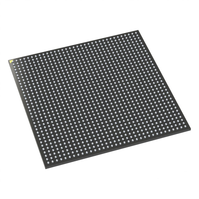
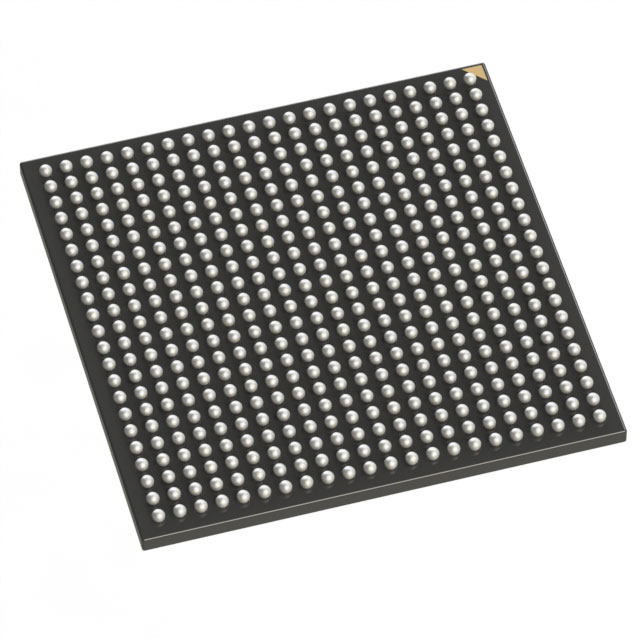
Overview of M2GL150-FCS536I – IGLOO2 Field Programmable Gate Array (FPGA), 146,124 logic elements
The M2GL150-FCS536I is an IGLOO2 Field Programmable Gate Array (FPGA) IC from Microchip Technology offering 146,124 logic elements and approximately 5.12 Mbits of embedded memory. It provides a high-density logic fabric with 293 user I/O pins and a compact 536-LFBGA (536-CSPBGA, 16×16) package for surface-mount assembly.
Designed for industrial-grade deployments, the device supports a wide supply range and extended operating temperature range, making it suitable for systems that require substantial on-chip logic, memory, and flexible I/O in a space-efficient package.
Key Features
- Logic Capacity 146,124 logic elements provide substantial programmable logic resources for complex combinational and sequential functions.
- Embedded Memory Approximately 5.12 Mbits of on-chip RAM to support data buffering, state storage, and intermediate processing without requiring external memory for many use cases.
- I/O Count 293 user I/O pins enable dense connectivity to peripherals, sensors, and board-level interfaces.
- Power Supply Flexibility Supported voltage supply range from 1.14 V to 2.625 V to accommodate varied core and I/O power domain requirements.
- Package and Mounting 536-LFBGA / 536-CSPBGA (16×16) package in a surface-mount form factor for compact board integration.
- Industrial Temperature Grade Rated for operation from −40 °C to 100 °C for deployment in temperature-challenging environments.
- RoHS Compliant Conforms to RoHS environmental requirements for lead-free assembly and regulatory compliance.
Typical Applications
- High-density I/O control: Use where hundreds of GPIOs are needed to interface with boards, peripherals, or complex sensor arrays, leveraging 293 available I/Os.
- On-chip data buffering and processing: Implement data paths and temporary storage using approximately 5.12 Mbits of embedded RAM to reduce external memory requirements.
- Complex logic consolidation: Replace multiple discrete logic devices with a single FPGA using 146,124 logic elements to simplify board-level design.
- Industrial systems and equipment: Suitable for designs requiring industrial-grade temperature performance (−40 °C to 100 °C) and surface-mount packaging.
Unique Advantages
- High logic density: 146,124 logic elements enable implementation of large state machines, datapaths, and custom logic blocks on a single device.
- Substantial embedded memory: Approximately 5.12 Mbits of on-chip RAM reduces dependence on external memory and tightens system integration.
- Extensive I/O capability: 293 I/O pins provide flexibility for parallel interfaces, control signals, and mixed I/O architectures.
- Wide supply voltage range: 1.14 V to 2.625 V support for diverse power-domain strategies and compatibility with multiple logic levels.
- Industrial temperature rating: −40 °C to 100 °C operation addresses thermal requirements for hardened and constrained environments.
- Compact BGA packaging: 536-LFBGA / 536-CSPBGA package delivers a high pin count in a small footprint for space-constrained boards.
Why Choose M2GL150-FCS536I?
The M2GL150-FCS536I positions itself as a high-capacity IGLOO2 FPGA option from Microchip Technology, combining a large number of logic elements with multi-megabit embedded RAM and a high I/O count in a compact BGA package. Its supported voltage range and industrial temperature grading make it a practical choice for designs that require robust, integrated programmable logic in demanding environments.
This device is suited for engineers and teams seeking to consolidate logic, reduce external components, and maintain design flexibility while keeping form-factor and thermal requirements in mind. Its specification set supports scalable implementations where on-chip resources and reliable operation across a broad temperature range are priorities.
If you would like pricing, availability, or to request a quote for the M2GL150-FCS536I, please submit a quote request or contact sales for further assistance.


Date Founded: 1989
Headquarters: Chandler, Arizona, USA
Employees: 22,000+
Revenue: $8.349 Billion
Certifications and Memberships: ISO9001:2015, IATF16949:2016, AS 9100D


