
JS27HP2G08SDDA-45
| Part Description |
2K page 4-bit ECC 128 byte spare |
|---|---|
| Quantity | 629 Available (as of June 17, 2026) |

| Product Category | Flash Memory |
|---|---|
| Manufacturer | Jeju Semiconductor Corporation |
| Manufacturing Status | Mass Production |
| Manufacturer Standard Lead Time | Contact Us |
| Datasheet |
Specifications & Environmental
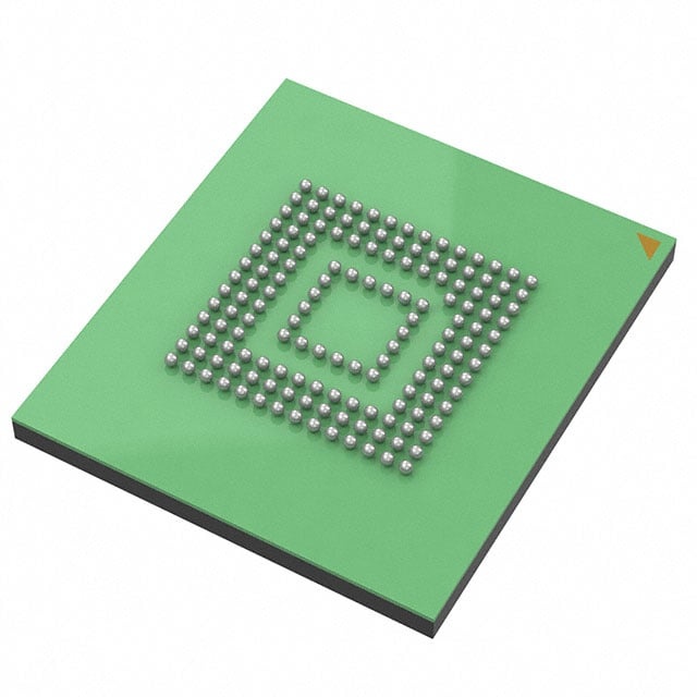
| Device Package | 63-BGA (9.0x11.0mm) | Memory Format | FLASH | Technology | FLASH - NAND (SLC) | ||
|---|---|---|---|---|---|---|---|
| Memory Size | 2 Gbit | Access Time | 45 ns | Grade | Industrial | ||
| Clock Frequency | 22.22 MHz | Voltage | 1.8V | Memory Type | Non-Volatile | ||
| Operating Temperature | -40°C - 85°C | Write Cycle Time Word Page | 300 µs | Mounting Method | Surface Mount | ||
| Memory Interface | Parallel | Memory Organization | x8 | Moisture Sensitivity Level | 3 | ||
| RoHS Compliance | Compliant | ECCN | EAR99 | HTS Code | 8542.32.00.71 |
Overview of JS27HP2G08SDDA-45 – 2K page 4-bit ECC 128 byte spare
The JS27HP2G08SDDA-45 is a 2 Gbit SLC NAND Flash memory organized as x8 with a 2K page and 128-byte spare area, designed for non-volatile embedded storage in industrial applications. It provides a parallel NAND interface with 4-bit ECC, low-voltage 1.8V operation, and a compact 63-ball FBGA package optimized for surface-mount assembly.
This device is targeted at mass storage and embedded firmware/data logging applications where robust endurance, on-device ECC and industrial temperature operation are required. Key value propositions include on-chip ECC support, proven NAND block architecture, and specifications tuned for reliable solid-state storage in industrial environments.
Key Features
- Memory Core 2 Gbit SLC NAND Flash organized as x8 with 2K page size and a 128-byte spare area for metadata and ECC.
- On‑chip ECC & Reliability 4-bit ECC implemented per 528 bytes (x8) to improve data integrity; specified 10 years typical data retention and 100,000 program/erase cycles for the industrial temperature range.
- Performance 45 ns sequential access (1.8V device), 300 µs typical page program time and 3.5 ms typical block erase time for 2 Gbit devices, supporting high-throughput page operations.
- Interface & Timing Parallel NAND interface with x8 I/O and support for fast cache read and copy‑back programming to accelerate internal data movement.
- Power Low-voltage operation at nominal 1.8V (Vcc range 1.7 V–1.95 V for 1.8V device variants) to meet modern low-power system requirements.
- Package & Mounting 63-ball FBGA surface-mount package (9.0 × 11.0 × 1.0 mm footprint) for compact board integration and reliable soldered connections.
- Operating Range Industrial temperature grade rated from −40°C to 85°C suitable for a wide range of embedded and industrial environments.
- Standards & Features ONFI 1.0 compliant command set, status register reporting, hardware data protection during power transitions, and simple chip‑enable behavior for MCU integration.
- Compliance RoHS-compliant construction (lead-free & halogen-free options indicated in series documentation).
Typical Applications
- Industrial Embedded Storage Local non-volatile data and firmware storage in controllers, PLCs and instrumentation where industrial temperature operation and high endurance are required.
- Mass Storage for Consumer/Pro‑grade Devices Page- and block-oriented data storage for solid-state mass storage applications that benefit from SLC endurance and on-chip ECC.
- Data Logging & Telemetry Reliable long-term data capture and retention in remote or harsh environments thanks to SLC endurance and 10-year typical data retention.
- Firmware & Boot Flash Compact, surface-mount NAND for storing firmware images with ECC protection and fast page program/read characteristics.
Unique Advantages
- High Endurance SLC NAND: 100,000 program/erase cycles specified over the industrial temperature range supports frequent updates and long operational life.
- On‑Device ECC: 4-bit ECC per 528 bytes reduces host-side error-handling complexity and enhances data integrity without extra external components.
- Low-Voltage Operation: 1.8V supply reduces system power budget and simplifies integration into modern low-voltage platforms.
- Compact, Industry-Friendly Package: 63-ball FBGA (9.0 × 11.0 mm) enables small board area and robust surface-mount assembly for space-constrained designs.
- Fast Page and Block Operations: 45 ns sequential read timing and 300 µs typical page program time accelerate read/write cycles for page-oriented workloads.
- Industrial Temperature Support: Certified for −40°C to 85°C operation, allowing deployment across a broad range of field and industrial environments.
Why Choose JS27HP2G08SDDA-45?
The JS27HP2G08SDDA-45 combines SLC NAND endurance, on-chip 4-bit ECC and low-voltage 1.8V operation in a compact 63-ball FBGA package tailored for industrial embedded storage. Its page and block performance characteristics, together with proven NAND features such as copy-back programming and cache read, make it suitable for designs that require robust, long-life non-volatile memory with integrated data integrity features.
This part is well suited to engineers and procurement teams designing industrial controllers, data loggers, firmware storage solutions and other embedded systems that demand reliable NAND flash with transparent ECC handling and compact board integration.
Request a quote or submit an inquiry to begin evaluating the JS27HP2G08SDDA-45 for your next embedded storage design.


Date Founded: 2000
Headquarters: Jeju-si, Jeju-do, Republic of Korea
Employees: 100+
Revenue: $100 Million
Certifications and Memberships: ISO9001:2015, ISO14001:2015, AEC-Q100, RoHS, REACH


