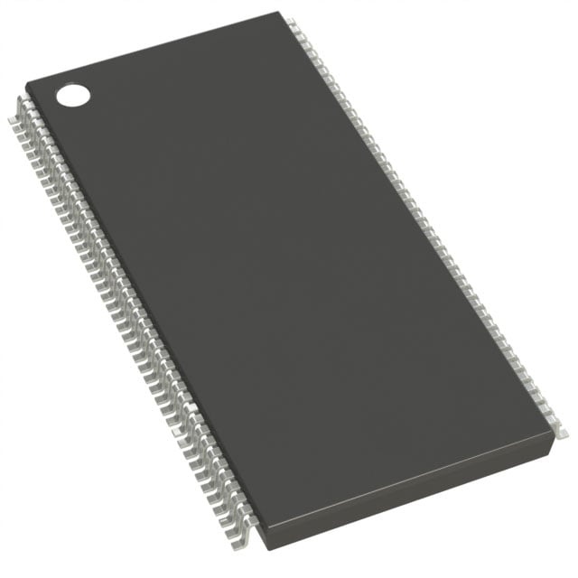
IS42S32400J-7TLI
| Part Description |
IC DRAM 128MBIT PAR 86TSOP II |
|---|---|
| Quantity | 634 Available (as of June 13, 2026) |
| Product Category | Memory |
|---|---|
| Manufacturer | Integrated Silicon Solution Inc |
| Manufacturing Status | Active |
| Manufacturer Standard Lead Time | 14 Weeks |
| Datasheet |
Specifications & Environmental
| Device Package | 86-TSOP II | Memory Format | DRAM | Technology | SDRAM | ||
|---|---|---|---|---|---|---|---|
| Memory Size | 128 Mbit | Access Time | 5.4 ns | Grade | Industrial | ||
| Clock Frequency | 143 MHz | Voltage | 3V ~ 3.6V | Memory Type | Volatile | ||
| Operating Temperature | -40°C ~ 85°C (TA) | Write Cycle Time Word Page | N/A | Packaging | 86-TFSOP (0.400", 10.16mm Width) | ||
| Mounting Method | Volatile | Memory Interface | LVTTL | Memory Organization | 4M x 32 | ||
| Moisture Sensitivity Level | 3 (168 Hours) | RoHS Compliance | ROHS Compliant | REACH Compliance | REACH Unaffected | ||
| Qualification | N/A | ECCN | EAR99 | HTS Code | 8542.32.0002 |
Overview of IS42S32400J-7TLI - 128Mbit SDRAM Memory IC
The IS42S32400J-7TLI is a 128-megabit synchronous dynamic random-access memory (SDRAM) integrated circuit from ISSI, Integrated Silicon Solution Inc. Organized as 4M x 32, this volatile memory device operates at clock frequencies up to 143 MHz with a 5.4 nanosecond access time. Designed for industrial applications requiring reliable memory solutions, the IS42S32400J-7TLI provides cost-effective storage with an extended operating temperature range of -40°C to 85°C.
This parallel DRAM is housed in an 86-pin TSOP II package, offering a proven form factor for PCB designs where space efficiency and thermal management are important. With a standard LVTTL interface and 3V to 3.6V supply voltage, the IS42S32400J-7TLI integrates easily into existing digital systems requiring high-bandwidth memory access.
Key Features
- Memory Architecture - 128 Mbit capacity organized as 4M x 32, providing flexible data width for 32-bit bus architectures with straightforward address decoding.
- Performance Specifications - 143 MHz clock frequency with 5.4 ns access time delivers consistent throughput for real-time processing applications that require predictable memory performance.
- Power Supply - 3V to 3.6V operating voltage range supports common digital system power rails, simplifying power distribution design and reducing the need for dedicated regulators.
- Interface Standard - LVTTL-compatible signals enable direct connection to microcontrollers, DSPs, and FPGAs without level shifting, reducing component count and board complexity.
- Package Type - 86-pin TSOP II package in 10.16mm width provides a mature, well-characterized footprint with established PCB layout guidelines and wide assembly process compatibility.
- Temperature Range - -40°C to 85°C ambient operating temperature extends reliability across industrial environments where thermal conditions vary beyond standard commercial limits.
Typical Applications
- Industrial Control Systems - This SDRAM serves as working memory in programmable logic controllers (PLCs) and distributed control systems where the extended temperature range ensures stable operation in factory floor and process control installations.
- Embedded Computing Platforms - The device provides main system RAM for single-board computers and embedded processors used in industrial automation, where 128 Mbit capacity accommodates operating systems and application code for mid-range processing tasks.
- Data Acquisition Systems - The 32-bit organization and 143 MHz operation support high-speed data buffering in instrumentation and measurement equipment, where consistent access times prevent data loss during rapid sampling operations.
- Telecommunications Infrastructure - This memory IC functions in base stations and network switching equipment operating in temperature-controlled but non-climate-conditioned environments, where the industrial temperature rating provides margin beyond standard commercial components.
- Medical Equipment - The SDRAM provides data storage for diagnostic instruments and patient monitoring systems where reliable operation across varying ambient temperatures is required in clinical and mobile healthcare settings.
Unique Advantages
- Streamlined System Architecture: The 4M x 32 organization matches common 32-bit processor buses directly, eliminating the need for memory interleaving or bank switching logic that would increase PCB area and design complexity.
- Reduced Bill of Materials Cost: LVTTL interface compatibility removes voltage level translators and additional support components, lowering total system cost while simplifying layout and reducing potential failure points.
- Extended Environmental Reliability: The -40°C to 85°C operating range provides headroom beyond typical commercial specifications, reducing field failures in installations where temperature control is limited or seasonal variations occur.
- Proven Package Technology: TSOP II packaging offers mature assembly processes with extensive manufacturer experience, resulting in predictable yields and lower production risk compared to newer, higher-density package types.
- Design Reuse Opportunity: Standard SDRAM command structure and timing align with widely-used memory controllers in microprocessors and FPGAs, allowing designers to leverage existing reference designs and reduce development time.
- Long-Term Availability: Active lifecycle status from ISSI indicates ongoing production support, providing confidence for product designs requiring multi-year component availability for spares and manufacturing continuity.
Why Choose IS42S32400J-7TLI?
The IS42S32400J-7TLI addresses the needs of industrial and embedded system designers who require reliable memory performance without the complexity or cost premium of specialized memory technologies. Its combination of standard interfaces, proven packaging, and extended temperature operation makes it suitable for applications where environmental conditions exceed commercial limits but do not require fully ruggedized or military-grade components. The 128 Mbit density provides adequate capacity for many embedded operating systems and real-time applications while maintaining a manageable PCB footprint.
For design teams prioritizing component longevity and supply chain stability, the active lifecycle status and TSOP II package format offer advantages in long-production-run products. The device's straightforward integration requirements reduce time-to-market for systems where memory subsystem design can leverage standard controller IP and reference schematics, allowing engineering resources to focus on application-specific functionality rather than low-level memory interface development.
Request a Quote
For pricing information, volume availability, and technical support on the IS42S32400J-7TLI, contact our sales team. We can assist with inventory planning, provide guidance on PCB layout considerations, and help evaluate this SDRAM's fit for your specific application requirements.