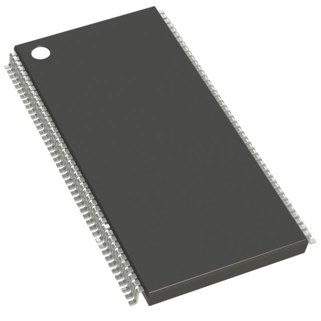
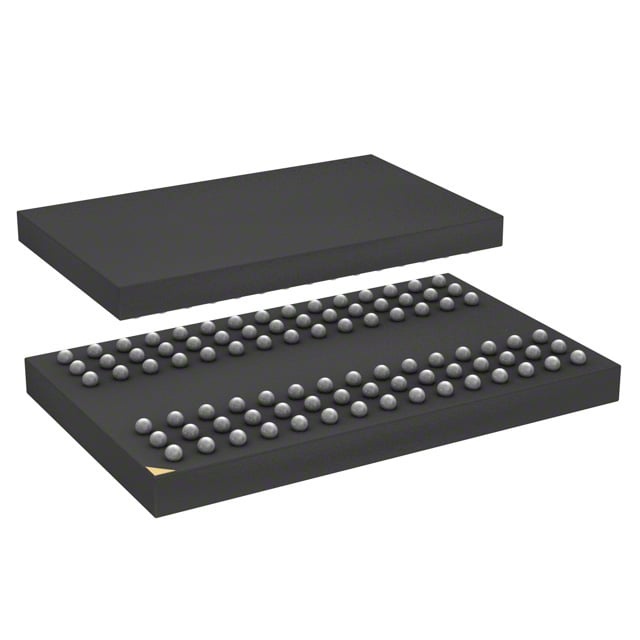
IS42S32800B-6BL
| Part Description |
IC DRAM 256MBIT PAR 90TFBGA |
|---|---|
| Quantity | 935 Available (as of June 17, 2026) |

| Product Category | DRAM Memory |
|---|---|
| Manufacturer | Integrated Silicon Solution Inc |
| Manufacturing Status | Obsolete |
| Manufacturer Standard Lead Time | Contact Us |
| Datasheet |
Specifications & Environmental
| Device Package | 90-TFBGA (8x13) | Memory Format | DRAM | Technology | SDRAM | ||
|---|---|---|---|---|---|---|---|
| Memory Size | 256 Mbit | Access Time | 5.5 ns | Grade | Commercial | ||
| Clock Frequency | 166 MHz | Voltage | 3V ~ 3.6V | Memory Type | Volatile | ||
| Operating Temperature | 0°C ~ 70°C (TA) | Write Cycle Time Word Page | N/A | Packaging | 90-TFBGA | ||
| Mounting Method | Volatile | Memory Interface | Parallel | Memory Organization | 8M x 32 | ||
| Moisture Sensitivity Level | 3 (168 Hours) | RoHS Compliance | ROHS3 Compliant | REACH Compliance | REACH Unaffected | ||
| Qualification | N/A | ECCN | EAR99 | HTS Code | 8542.32.0024 |
Overview of IS42S32800B-6BL – IC DRAM 256MBIT PAR 90TFBGA
The IS42S32800B-6BL is a 256‑Mbit synchronous DRAM (SDRAM) device organized as 8M × 32 (quad banks of 2M × 32) with a parallel memory interface. It implements a fully synchronous, pipelined architecture with programmable burst and mode options to support high‑bandwidth memory access patterns.
Typical use cases include systems that require high memory throughput in a compact package — offering configurable latency and burst behavior for integration into memory subsystems and embedded equipment operating from a 3.0–3.6 V supply and 0 °C to 70 °C ambient.
Key Features
- Synchronous SDRAM Core Fully synchronous operation with internal pipelined architecture and four internal banks (2M × 32 bits × 4 banks) for parallel access and predictable timing.
- High Clock Rate and Timing Supports clock rates of 166 MHz (also 143 MHz) with CAS latency selectable at 2 or 3 and an access time of 5.5 ns.
- Flexible Burst and Mode Control Programmable burst lengths of 1, 2, 4, 8 or full page, with interleaved or linear burst types and burst‑stop functionality; programmable mode register for tailored operation.
- Auto and Self Refresh Supports Auto Refresh and Self Refresh modes with 4096 refresh cycles/64 ms (and 4096/32 ms for industrial grade) to maintain data integrity during standby.
- Byte Masking and Data Control Individual byte control via DQM0–DQM3 for masked writes and controlled data outputs.
- Power and Interface Single +3.3 V ±0.3 V supply (3.0–3.6 V) with LVTTL interface signals and CKE support for power-down/self-refresh entry; input buffers disabled during low‑power modes to reduce standby power.
- Package and Thermal Available in 90‑TFBGA (8 × 13, 90‑ball, 0.8 mm ball pitch) package; specified operating ambient temperature 0 °C to 70 °C.
- Additional Functional Support Concurrent auto precharge, burst‑read/single‑write operation, and bank select inputs (BS0/BS1) for per‑bank command targeting.
Typical Applications
- High‑bandwidth memory subsystems — Used where sustained burst transfers and pipelined synchronous accesses are required to meet throughput demands.
- Embedded systems — Compact BGA package and configurable timing suit space‑constrained designs requiring parallel SDRAM.
- Memory buffering and caching — Programmable burst lengths and byte‑level data masking support efficient buffer and cache implementations.
Unique Advantages
- Configurable Performance Modes: Programmable CAS latency, burst lengths and burst type allow tuning for different access patterns and system timing.
- Quad‑Bank Architecture: Four internal banks (2M × 32 each) enable interleaved access and improved effective concurrency for burst operations.
- Byte‑level Control: Individual DQM0–DQM3 signals provide masked write capability and precise output control for multi‑byte transactions.
- Low‑power Standby Behavior: CKE‑controlled power‑down and self‑refresh modes, with input buffers disabled, reduce standby power when banks are idle.
- Compact BGA Packaging: 90‑TFBGA (8×13, 0.8 mm pitch) offers a small footprint for dense board designs.
Why Choose IS42S32800B-6BL?
The IS42S32800B-6BL provides a synchronous, pipelined DRAM architecture with flexible timing and burst configuration to address designs needing predictable, high‑throughput parallel memory. Its quad‑bank organization, byte masking, and selectable CAS latency make it suitable for systems that require configurable performance and efficient burst transfers.
Available in a compact 90‑TFBGA package and operating from a standard 3.3 V supply within a 0 °C to 70 °C range, this device fits board‑level memory subsystems where space and deterministic timing are important.
For pricing, lead time or to request a quote for IS42S32800B-6BL, please submit your request to obtain a formal quotation and availability information.