IS42S32800B-6BLI
| Part Description |
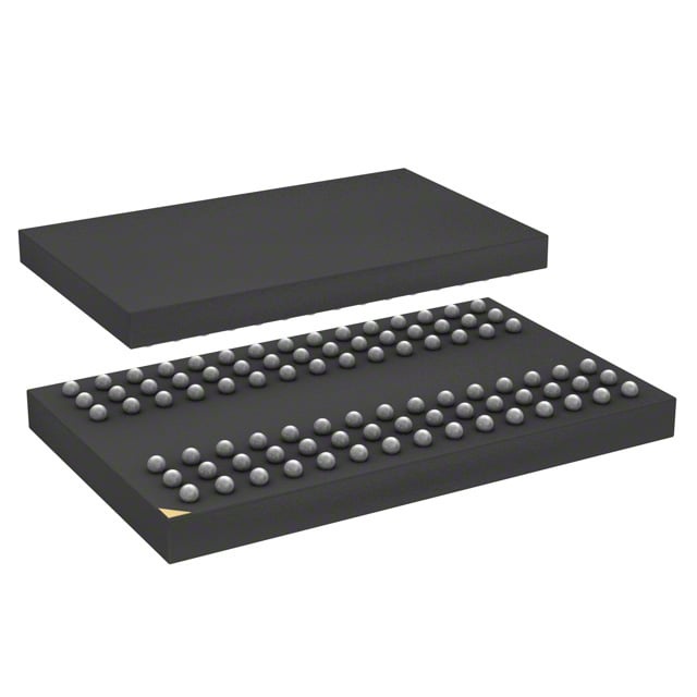
IC DRAM 256MBIT PAR 90TFBGA |
|---|---|
| Quantity | 408 Available (as of June 15, 2026) |

| Product Category | Memory |
|---|---|
| Manufacturer | Integrated Silicon Solution Inc |
| Manufacturing Status | Obsolete |
| Manufacturer Standard Lead Time | Contact Us |
| Datasheet |
Specifications & Environmental
| Device Package | 90-TFBGA (8x13) | Memory Format | DRAM | Technology | SDRAM | ||
|---|---|---|---|---|---|---|---|
| Memory Size | 256 Mbit | Access Time | 5.5 ns | Grade | Industrial | ||
| Clock Frequency | 166 MHz | Voltage | 3V ~ 3.6V | Memory Type | Volatile | ||
| Operating Temperature | -40°C ~ 85°C (TA) | Write Cycle Time Word Page | N/A | Packaging | 90-TFBGA | ||
| Mounting Method | Volatile | Memory Interface | Parallel | Memory Organization | 8M x 32 | ||
| Moisture Sensitivity Level | 3 (168 Hours) | RoHS Compliance | ROHS Compliant | REACH Compliance | REACH Unaffected | ||
| Qualification | N/A | ECCN | EAR99 | HTS Code | 8542.32.0024 |
Overview of IS42S32800B-6BLI – IC DRAM 256MBIT PAR 90TFBGA
The IS42S32800B-6BLI is a 256‑Mbit synchronous DRAM organized as 8M × 32 with four internal banks, implemented in a pipelined architecture. It provides a fully synchronous parallel memory interface with programmable burst modes and timing options to support designs that require predictable, high-bandwidth memory access.
This device targets systems that need a 3.3 V ±0.3 V SDRAM solution with operating range −40 °C to 85 °C, delivered in a 90‑TFBGA (8×13) package for compact board integration.
Key Features
- Core / Memory Architecture Quad-bank organization (2M × 32 bits × 4 banks) providing a total 256‑Mbit capacity and internal pipelined architecture for efficient command sequencing.
- Performance Clock rate options at 166/143 MHz, CAS latency selectable at 2 or 3, and access time specified at 5.5 ns for timing-sensitive designs.
- Burst and Mode Control Programmable burst lengths of 1, 2, 4, 8 or full page, with linear or interleaved burst types, burst‑read/single‑write support and burst termination.
- Refresh and Power Auto Refresh and Self Refresh supported with 4096 refresh cycles/64 ms (and 4096/32 ms for industrial grade); CKE-controlled clock enable for Power Down and Self Refresh handling.
- Byte Control and Commands Individual byte masking via DQM0–DQM3, concurrent auto precharge, and programmable mode register to select operating modes.
- Interface and Voltage LVTTL interface, parallel memory interface, and single +3.3 V ±0.3 V supply (specified 3.0 V to 3.6 V).
- Package and Temperature 90‑ball LF‑BGA (90‑TFBGA, 8×13 mm, 0.8 mm ball pitch) package and supported operating temperature range of −40 °C to 85 °C.
Typical Applications
- High‑bandwidth systems — Use where sustained memory throughput is required; programmable burst modes and pipelined operation optimize sequential access.
- Synchronous DRAM designs — Integrates with systems that use registered clocked interfaces and LVTTL signaling for predictable timing behavior.
- Industrial‑temperature equipment — Suitable for designs that require operation across −40 °C to 85 °C with standard refresh options for reliability.
- Compact board implementations — 90‑TFBGA package supports space‑constrained layouts while providing 256‑Mbit capacity.
Unique Advantages
- Flexible burst control: Programmable burst lengths and burst type options allow tailoring memory transactions to application access patterns.
- Multiple timing choices: Support for 166/143 MHz clock rates and CAS latencies of 2 or 3 enables tradeoffs between latency and throughput.
- Banked architecture for concurrency: Four internal banks (2M × 32 each) facilitate interleaved accesses and improve effective bandwidth for multi‑threaded or pipelined workloads.
- Robust refresh modes: Auto and Self Refresh with defined refresh cycle rates, plus CKE control, help manage power and data integrity across operating modes.
- Byte‑level control: Individual DQM0–DQM3 byte masking supports partial‑width writes and fine‑grained data handling.
- Compact, board‑friendly package: 90‑TFBGA (8×13 mm) offers a small footprint for high‑density designs while delivering standard BGA mounting.
Why Choose IS42S32800B-6BLI?
The IS42S32800B-6BLI delivers a synchronous, pipelined 256‑Mbit DRAM solution with flexible burst modes, selectable CAS latency, and a quad‑bank architecture that together enable predictable high‑bandwidth performance. Its LVTTL interface and +3.3 V supply compatibility make it suitable for systems designed around standard SDRAM signaling.
Designed for engineers and procurement seeking a compact 90‑TFBGA package with industrial temperature capability, this device is appropriate for applications that need reliable, configurable SDRAM behavior with supported refresh and power control features.
Request a quote or submit an inquiry to obtain pricing, availability, and ordering information for IS42S32800B-6BLI.