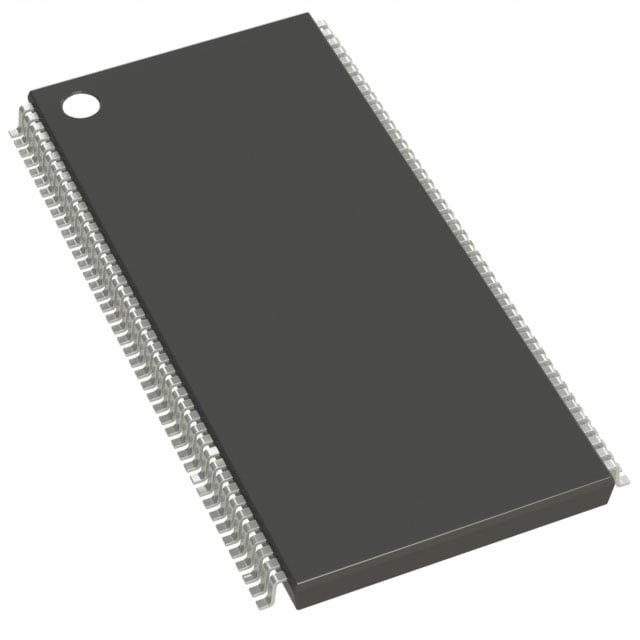
IS42S32800B-6TL
| Part Description |
IC DRAM 256MBIT PAR 86TSOP II |
|---|---|
| Quantity | 473 Available (as of June 15, 2026) |

| Product Category | Memory |
|---|---|
| Manufacturer | Integrated Silicon Solution Inc |
| Manufacturing Status | Obsolete |
| Manufacturer Standard Lead Time | Contact Us |
| Datasheet |
Specifications & Environmental
| Device Package | 86-TSOP II | Memory Format | DRAM | Technology | SDRAM | ||
|---|---|---|---|---|---|---|---|
| Memory Size | 256 Mbit | Access Time | 5.5 ns | Grade | Commercial | ||
| Clock Frequency | 166 MHz | Voltage | 3V ~ 3.6V | Memory Type | Volatile | ||
| Operating Temperature | 0°C ~ 70°C (TA) | Write Cycle Time Word Page | N/A | Packaging | 86-TFSOP (0.400", 10.16mm Width) | ||
| Mounting Method | Volatile | Memory Interface | Parallel | Memory Organization | 8M x 32 | ||
| Moisture Sensitivity Level | 3 (168 Hours) | RoHS Compliance | ROHS3 Compliant | REACH Compliance | REACH Unaffected | ||
| Qualification | N/A | ECCN | EAR99 | HTS Code | 8542.32.0024 |
Overview of IS42S32800B-6TL – IC DRAM 256MBIT PAR 86TSOP II
The IS42S32800B-6TL is a 256‑Mbit synchronous dynamic RAM (SDRAM) implemented as four internal 2M × 32‑bit banks, delivering a total organization of 8M × 32. It features a fully synchronous, pipelined architecture with a parallel LVTTL interface and supports clock rates up to 166 MHz for high‑bandwidth memory access.
This device is designed for systems that require flexible burst operation, programmable latency and refresh control. Key value propositions include high sustained throughput via internal banking and burst modes, configurable timing (CAS latency 2 or 3), and compact 86‑pin TSOP II packaging for board‑level integration.
Key Features
- Core Architecture Quad configuration of 2M × 32 bits per bank (4 banks) yielding 256‑Mbit total; fully synchronous operation with internal pipelined architecture.
- Memory Organization Organized as 4096 rows × 512 columns × 32 bits per bank supporting burst‑read and single‑write operations.
- Performance Supports clock rates of 166/143 MHz and access time down to 5.5 ns; CAS latency selectable at 2 or 3 to match system timing needs.
- Burst and Mode Flexibility Programmable burst lengths (1, 2, 4, 8, or full page) and burst type (interleaved or linear) with burst stop and burst‑terminate functionality.
- Refresh and Power Control Auto Refresh and Self Refresh supported; 4096 refresh cycles/64 ms (15.6 μs/row), with power‑down and self‑refresh modes for reduced standby power.
- Byte‑Level Masking Individual byte control via DQM0–DQM3 for write‑mask and output masking operations.
- Supply and Interface Single +3.3 V ±0.3 V power supply (3.0–3.6 V) and LVTTL I/O signaling.
- Package and Temperature Available in 86‑pin TSOP‑II (10.16 mm width) package; specified operating temperature range 0 °C to 70 °C (TA).
Typical Applications
- High‑bandwidth systems Suited for designs that require sustained memory throughput thanks to internal banking, pipelining and high clock rates.
- Synchronous memory subsystems Useful where fully synchronous operation and programmable burst behavior are needed to align with system timing and data flow.
- Buffering and burst‑transfer applications Applicable for use cases that benefit from selectable burst lengths and CAS latency to optimize transfer efficiency.
Unique Advantages
- Programmable performance modes: CAS latency selectable at 2 or 3 and multiple burst lengths allow tuning latency and throughput to application requirements.
- High throughput architecture: Internal pipelined design and four internal banks enable concurrent operations and improved effective bandwidth.
- Flexible refresh management: Supports Auto Refresh and Self Refresh with standard 4096‑cycle refresh intervals to maintain data integrity while managing power.
- Byte‑level control: DQM0–DQM3 provide per‑byte masking for finer control over write and output operations.
- Board‑friendly package: 86‑pin TSOP‑II (10.16 mm width) offers a compact footprint for system integration.
- Standard 3.3 V supply: Operates from a single +3.3 V ±0.3 V supply (3.0–3.6 V) for compatibility with common system rails.
Why Choose IS42S32800B-6TL?
The IS42S32800B-6TL delivers a configurable and synchronous 256‑Mbit DRAM solution that balances high data throughput, programmable latency and flexible burst operation. Its quad‑bank, pipelined architecture and LVTTL interface make it suitable for designs that demand predictable timing and sustained memory bandwidth.
This device is well suited for designers seeking a compact, parallel SDRAM component with selectable operating modes, robust refresh control and standard 3.3 V supply compatibility. It provides long‑term design value through configurable performance parameters and common package options for board‑level integration.
Request a quote or submit an inquiry to our sales team to discuss availability, pricing and technical fit for your design.