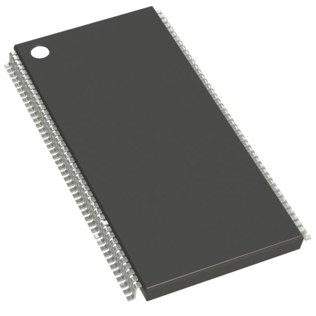
IS42S32800B-6TLI
| Part Description |
IC DRAM 256MBIT PAR 86TSOP II |
|---|---|
| Quantity | 224 Available (as of June 11, 2026) |

| Product Category | Memory |
|---|---|
| Manufacturer | Integrated Silicon Solution Inc |
| Manufacturing Status | Obsolete |
| Manufacturer Standard Lead Time | Contact Us |
| Datasheet |
Specifications & Environmental
| Device Package | 86-TSOP II | Memory Format | DRAM | Technology | SDRAM | ||
|---|---|---|---|---|---|---|---|
| Memory Size | 256 Mbit | Access Time | 5.5 ns | Grade | Industrial | ||
| Clock Frequency | 166 MHz | Voltage | 3V ~ 3.6V | Memory Type | Volatile | ||
| Operating Temperature | -40°C ~ 85°C (TA) | Write Cycle Time Word Page | N/A | Packaging | 86-TFSOP (0.400", 10.16mm Width) | ||
| Mounting Method | Volatile | Memory Interface | Parallel | Memory Organization | 8M x 32 | ||
| Moisture Sensitivity Level | 3 (168 Hours) | RoHS Compliance | ROHS3 Compliant | REACH Compliance | REACH Unaffected | ||
| Qualification | N/A | ECCN | EAR99 | HTS Code | 8542.32.0024 |
Overview of IS42S32800B-6TLI – IC DRAM 256MBIT PAR 86TSOP II
The IS42S32800B-6TLI is a 256-Mbit synchronous DRAM organized as quad 2M × 32-bit banks with a fully synchronous, pipelined architecture. It provides programmable burst lengths, selectable CAS latency, and features for auto and self refresh to support sustained, high-bandwidth memory access patterns.
Designed for applications requiring high memory throughput, the device operates from a single +3.3V supply and is available in an 86-pin TSOP-II package, delivering a combination of performance, configurable burst behavior, and a broad operating temperature range.
Key Features
- Core & Architecture Quad-bank organization: four internal banks of 2M × 32 bits (total 256 Mbit) with an internal pipelined architecture for efficient command sequencing.
- Performance Clock rate up to 166 MHz with CAS latency selectable at 2 or 3; access time specified at 5.5 ns for fast synchronous operation.
- Burst and Mode Flexibility Programmable burst lengths (1, 2, 4, 8, or full page) and burst type (interleaved or linear), plus a programmable mode register for tailored operation.
- Read/Write Control & Byte Masking Burst-Read/Single-Write support, burst stop, and individual byte control via DQM0–DQM3 for fine-grained data handling.
- Refresh and Power Control Auto Refresh and Self Refresh supported; 4096 refresh cycles/64 ms (15.6 μs/row) and 4096/32 ms option for industrial grade devices. CKE-driven clock enable for power-down control.
- Interface & Voltage Parallel memory interface with LVTTL signaling; single-supply operation at +3.3 V ±0.3 V (listed 3.0 V–3.6 V).
- Package & Temperature 86-pin TSOP-II (86-TFSOP listed) package with 0.50 mm pin pitch; package width notation includes 0.400" (10.16 mm). Operating temperature range: −40 °C to 85 °C (TA).
Typical Applications
- High-bandwidth memory subsystems — Provides synchronous, pipelined DRAM with high clock rates and burst capability for designs that require sustained transfer throughput.
- Embedded systems with parallel memory interfaces — Parallel LVTTL interface and byte masking support make it suitable for embedded platforms using synchronous DRAM.
- Systems requiring robust refresh control — Auto and Self Refresh modes and selectable refresh timing options support designs with varying standby and refresh requirements.
Unique Advantages
- High sustained transfer capability: Support for up to 166 MHz clocking and selectable CAS latency enables responsive synchronous operation for bandwidth-sensitive tasks.
- Flexible burst operation: Programmable burst lengths and burst type options allow tuning of read/write sequences to match system access patterns.
- Granular data control: Individual byte control via DQM0–DQM3 facilitates partial-word writes and selective data masking.
- Simplified power and refresh management: Auto and Self Refresh plus CKE-controlled power-down behavior help manage standby power and data retention needs.
- Wide operating range: Specified operation from −40 °C to 85 °C supports deployment in a broad set of environmental conditions.
- Standard supply and signaling: Single +3.3 V ±0.3 V supply and LVTTL interface ease integration into systems that use common DRAM voltage and logic levels.
Why Choose IS42S32800B-6TLI?
The IS42S32800B-6TLI combines a quad-bank, pipelined SDRAM architecture with selectable latency and flexible burst modes to address designs that demand synchronous, high-throughput memory. Its byte-level masking, refresh options, and single-supply operation simplify system design while enabling configurable performance.
This device is well suited for engineers designing systems that require predictable, high-bandwidth DRAM behavior and documented control over burst, refresh, and power modes. Detailed datasheet documentation for the IS42S32800B-6TLI supports evaluation and integration into target designs.
Request a quote or submit an inquiry to evaluate IS42S32800B-6TLI for your design and obtain pricing and availability information.