IS42S32800B-7BL
| Part Description |
IC DRAM 256MBIT PAR 90LFBGA |
|---|---|
| Quantity | 517 Available (as of June 15, 2026) |

| Product Category | Memory |
|---|---|
| Manufacturer | Integrated Silicon Solution Inc |
| Manufacturing Status | Obsolete |
| Manufacturer Standard Lead Time | Contact Us |
| Datasheet |
Specifications & Environmental
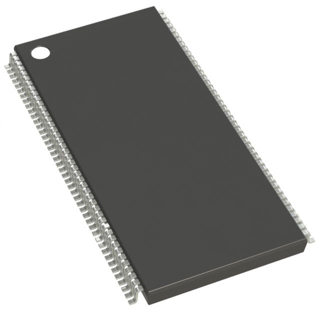
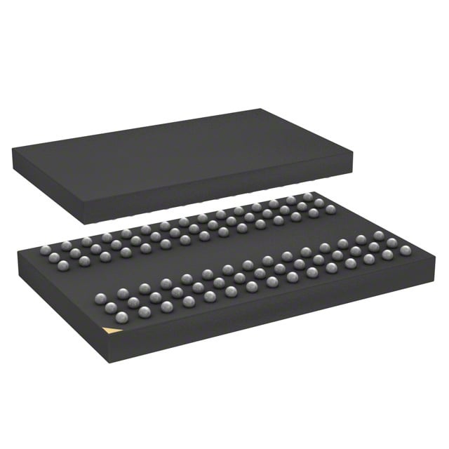
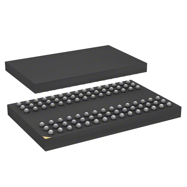
| Device Package | 90-LFBGA (8x13) | Memory Format | DRAM | Technology | SDRAM | ||
|---|---|---|---|---|---|---|---|
| Memory Size | 256 Mbit | Access Time | 5.5 ns | Grade | Commercial | ||
| Clock Frequency | 143 MHz | Voltage | 3V ~ 3.6V | Memory Type | Volatile | ||
| Operating Temperature | 0°C ~ 70°C (TA) | Write Cycle Time Word Page | N/A | Packaging | 90-LFBGA | ||
| Mounting Method | Volatile | Memory Interface | Parallel | Memory Organization | 8M x 32 | ||
| Moisture Sensitivity Level | 3 (168 Hours) | RoHS Compliance | ROHS Compliant | REACH Compliance | REACH Unaffected | ||
| Qualification | N/A | ECCN | EAR99 | HTS Code | 8542.32.0024 |
Overview of IS42S32800B-7BL – IC DRAM 256MBIT PAR 90LFBGA
The IS42S32800B-7BL is a 256‑Mbit synchronous DRAM organized as quad 2M × 32 banks with a fully synchronous, pipelined architecture. It implements a parallel SDRAM interface with programmable burst modes, CAS latency selection, and on‑die refresh functions to support high memory bandwidth requirements.
This device targets designs that require compact, high‑performance volatile memory implemented in a 90‑ball LF‑BGA package and powered from a single 3.0–3.6 V supply.
Key Features
- Core & Architecture – Quad bank organization (4 × 2M × 32) with internal pipelined architecture for concurrent operations and efficient command sequencing.
- Synchronous SDRAM Operation – Fully synchronous operation with clocked input sampling; supported clock rates include 166 MHz and 143 MHz and CAS latency options of 2 or 3.
- Burst Control – Programmable burst lengths (1, 2, 4, 8, or full page), selectable burst type (interleaved or linear), burst‑read/single‑write and burst‑stop functions for flexible data transfer patterns.
- Addressing & Bank Control – Bank select inputs and address inputs supporting row/column commands, auto precharge control and concurrent auto precharge capability.
- Refresh Management – Auto Refresh and Self Refresh support with 4096 refresh cycles/64 ms (15.6 µs/row); industrial option documented with 4096 refresh cycles/32 ms.
- Byte Masking – Individual byte control via DQM0–DQM3 for selective data masking during transfers.
- Performance & Timing – Access time specified at 5.5 ns; supports high throughput operation at the specified clock rates.
- Power & Interface – Single +3.3 V ±0.3 V supply (3.0–3.6 V) with LVTTL compatible interface signaling.
- Package – 90‑ball LF‑BGA (8 × 13 mm, 0.8 mm ball pitch) for compact PCB integration; Pb‑free package option available.
- Operating Temperature – Commercial temperature range: 0 °C to 70 °C (TA).
Typical Applications
- High‑bandwidth systems – Suited for designs that require sustained memory throughput where synchronous bursts and programmable CAS latency improve data transfer efficiency.
- Parallel SDRAM interfaces – Use in systems that employ parallel SDRAM signaling and require programmable burst lengths and banked memory access.
- Space‑constrained PCB designs – 90‑ball LF‑BGA (8 × 13 mm) package enables compact board layouts while providing 256‑Mbit density.
Unique Advantages
- Flexible burst and latency options: Programmable burst lengths and CAS latency (2 or 3) let designers tune performance for specific access patterns.
- Banked memory architecture: Four internal 2M × 32 banks support concurrent operations to improve effective memory bandwidth.
- Compact BGA packaging: 90‑ball LF‑BGA in an 8 × 13 mm footprint provides high density in a small form factor for space‑limited designs.
- Standard 3.3 V supply: Single +3.3 V ±0.3 V operation simplifies power rail requirements and system integration.
- Robust refresh control: Auto and Self Refresh with defined refresh cycle rates enable reliable data retention management.
Why Choose IS42S32800B-7BL?
The IS42S32800B-7BL combines a quad‑bank SDRAM architecture, programmable burst behavior and selectable CAS latency with a compact LF‑BGA package to deliver a balanced solution for systems requiring volatile, high‑throughput memory. Its supported clock rates, byte masking, and on‑die refresh features make it suitable for designs where controllable performance and integration density matter.
This device is appropriate for developers and procurement teams working on systems that need a 256‑Mbit synchronous DRAM with parallel interface, flexible timing options, and a 3.0–3.6 V power envelope, providing a clear specification foundation for integration and long‑term deployment.
Request a quote or submit an inquiry to get pricing and availability for the IS42S32800B-7BL and to discuss volume, packaging options, or lead‑time requirements.