IS42S32800B-7BI
| Part Description |
IC DRAM 256MBIT PAR 90LFBGA |
|---|---|
| Quantity | 627 Available (as of June 12, 2026) |
| Product Category | Memory |
|---|---|
| Manufacturer | Integrated Silicon Solution Inc |
| Manufacturing Status | Obsolete |
| Manufacturer Standard Lead Time | Contact Us |
| Datasheet |
Specifications & Environmental
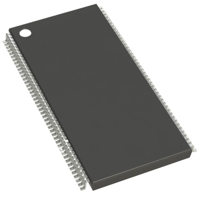
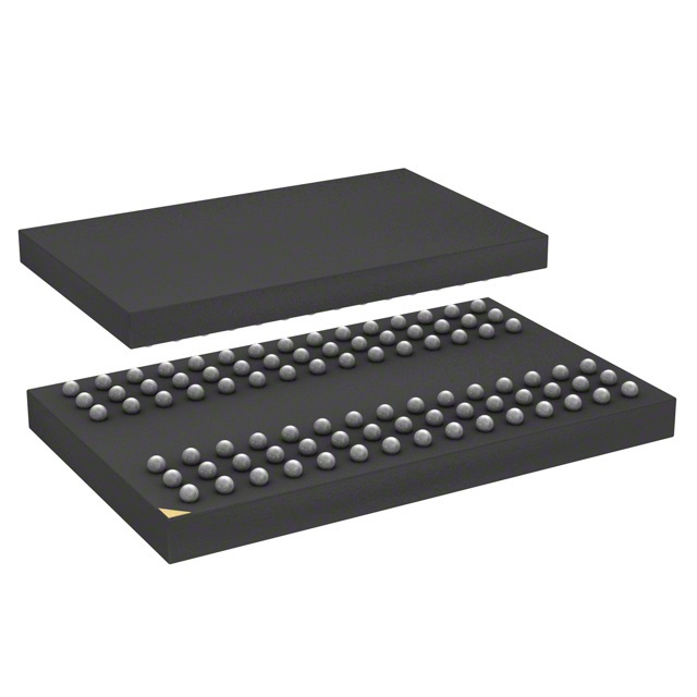
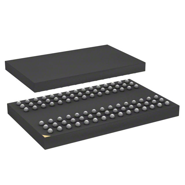
| Device Package | 90-LFBGA (8x13) | Memory Format | DRAM | Technology | SDRAM | ||
|---|---|---|---|---|---|---|---|
| Memory Size | 256 Mbit | Access Time | 5.5 ns | Grade | Industrial | ||
| Clock Frequency | 143 MHz | Voltage | 3V ~ 3.6V | Memory Type | Volatile | ||
| Operating Temperature | -40°C ~ 85°C (TA) | Write Cycle Time Word Page | N/A | Packaging | 90-LFBGA | ||
| Mounting Method | Volatile | Memory Interface | Parallel | Memory Organization | 8M x 32 | ||
| Moisture Sensitivity Level | 3 (168 Hours) | RoHS Compliance | ROHS3 Compliant | REACH Compliance | REACH Unaffected | ||
| Qualification | N/A | ECCN | EAR99 | HTS Code | 8542.32.0024 |
Overview of IS42S32800B-7BI – IC DRAM 256MBIT PAR 90LFBGA
The IS42S32800B-7BI is a 256‑Mbit synchronous DRAM (SDRAM) organized for parallel interface operation. It implements a pipelined, fully synchronous architecture with multiple internal banks to support burst access and high memory bandwidth workloads.
Targeted at systems that require high-throughput volatile memory, the device provides programmable burst lengths, selectable CAS latencies, and both auto and self‑refresh modes to balance performance and system-level control.
Key Features
- Memory Architecture 256‑Mbit DRAM organized as 2M × 32 × 4 banks (per datasheet) and also listed as 8M × 32 organization, supporting concurrent bank operation for improved throughput.
- Clock and Timing Clock rate options of 166 MHz and 143 MHz (per datasheet) with an access time of 5.5 ns and selectable CAS latency of 2 or 3.
- Burst and Mode Control Programmable burst lengths of 1, 2, 4, 8 or full page, with interleaved or linear burst types and burst‑read/single‑write support; programmable mode register for system optimization.
- Refresh and Power Modes Auto Refresh and Self Refresh supported. Standard refresh: 4096 cycles/64 ms; industrial‑grade option: 4096 cycles/32 ms (per datasheet).
- Byte Masking and I/O Individual byte control via DQM0–DQM3 and LVTTL input/output interface.
- Power Supply Single +3.3 V nominal supply with operating range 3.0 V to 3.6 V.
- Package and Mechanical 90‑ball LF‑BGA (8 × 13) package with 0.8 mm ball pitch; package option includes Pb‑free variant (per datasheet).
- Operating Range Specified operating temperature range from −40 °C to 85 °C (TA).
Typical Applications
- High‑Bandwidth Embedded Systems Used where burst transfers and pipelined synchronous access improve throughput for memory‑intensive tasks.
- Industrial Control and Instrumentation Operating temperature range and industrial refresh timing options support use in harsher environments.
- Synchronous Memory Subsystems Acts as parallel SDRAM in systems that require programmable burst and CAS modes to match system timing requirements.
Unique Advantages
- Configurable Performance: Selectable CAS latency (2 or 3) and programmable burst lengths let designers tune latency and throughput to match system needs.
- Concurrent Bank Architecture: Four internal banks enable overlapping operations to increase effective memory bandwidth.
- Synchronous Pipelined Design: Fully synchronous operation with internal pipelining supports predictable, clocked data transfers for system integration.
- Industrial‑Grade Options: Refresh timing and specified −40 °C to 85 °C operating range make the device suitable for temperature‑sensitive deployments.
- Compact BGA Packaging: 90‑ball LF‑BGA (8×13) provides a compact footprint for space‑constrained board designs; Pb‑free package option available.
- Byte‑Level Control: DQM0–DQM3 individual byte masking enables finer control over write masking and I/O handling.
Why Choose IS42S32800B-7BI?
The IS42S32800B-7BI combines a synchronous, pipelined SDRAM architecture with programmable timing and burst features to deliver a flexible 256‑Mbit memory option for designs that need predictable, high‑throughput parallel memory. Its four‑bank organization and selectable CAS/burst settings allow designers to optimize performance for a range of synchronous systems.
This device is suitable for engineers designing embedded and industrial systems that require a compact LF‑BGA package, configurable timing, and reliable refresh options across a wide operating temperature range.
If you would like pricing, lead‑time, or technical availability information, request a quote or submit an inquiry and our team will respond with details and support options.