
A31L214RL
| Part Description |
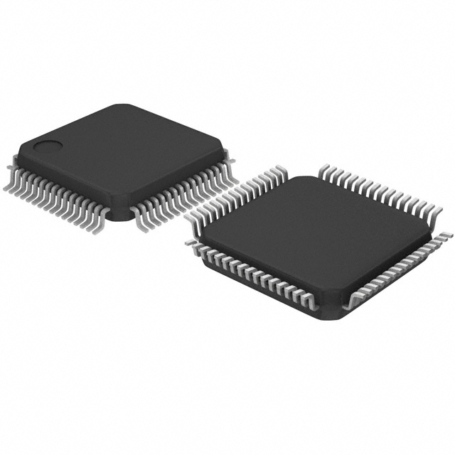
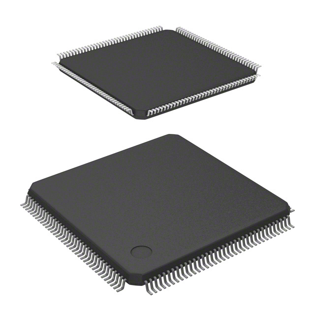
Abov A31L214RL ARM Cortex-M0+ 32-bit MCU — 128 Kbytes Flash, 20 Kbytes SRAM, 64-LQFP |
|---|---|
| Quantity | 949 Available (as of October 16, 2026) |

| Product Category | Microcontrollers |
|---|---|
| Manufacturer | ABOV Semiconductor |
| Manufacturing Status | Mass Production |
| Manufacturer Standard Lead Time | Contact Us |
| Datasheet |
Specifications & Environmental
| Connectivity | I2C, LPUART, SmartCard, SPI, UART/USART | Core Processor | ARM Cortex-M0+ | Core Size | 32-Bit | ||
|---|---|---|---|---|---|---|---|
| Data Converters | A/D 16x12b | Device Package | 64-LQFP | ECCN | 5A992.c | ||
| EEPROM Size | 4 Kbytes | HTS Code | 8542.31.00.00 | Moisture Sensitivity Level | N/A | ||
| Mounting Method | Surface Mount | Number of I/O | 57 | Operating Temperature | -40°C - 105°C | ||
| Oscillator Type | Internal/External | Package / Case | 64-LQFP | Program Memory Size | 128 Kbytes | ||
| Program Memory Type | FLASH | RAM Size | 20 Kbytes | REACH Compliance | Unknown | ||
| RoHS Compliance | Unknown | Speed | 32 MHz | Voltage | 1.71V - 3.6V |
Overview of A31L214RL – Abov A31L214RL ARM Cortex-M0+ 32-bit MCU — 128 Kbytes Flash, 20 Kbytes SRAM, 64-LQFP
The A31L214RL is an ultra-low power 32-bit microcontroller from Abov’s A31L21x series, built around an ARM Cortex-M0+ core and running up to 32 MHz. It integrates 128 Kbytes of Flash, 4 Kbytes of data flash and 20 Kbytes of SRAM alongside a broad set of peripherals for embedded and battery-powered systems.
Targeted at IoT nodes, smart meters, security and consumer devices, the A31L214RL combines extensive analog and digital interfaces, hardware security primitives and low-power modes to simplify system design and reduce BOM complexity.
Key Features
- Core — ARM Cortex-M0+ 32-bit core operating up to 32 MHz, with Nested Vector Interrupt Controller (NVIC) and SWD debug support for efficient real-time control and development.
- Memory — 128 Kbytes internal Flash, 4 Kbytes data Flash and 20 Kbytes SRAM plus a 32-byte backup register for code storage, data logging and fast runtime performance.
- Power and Supply — Wide operating supply 1.71 V to 3.6 V with integrated POR, LVR, LVI, internal RC oscillator and multiple sleep modes to support low-power applications.
- Low-power operation — Typical-run and deep-sleep currents documented: 90 μA/MHz in RUN; 0.99 μA in DEEP SLEEP with RTCC and retention; 0.35 μA in DEEP SLEEP with power control; 45 nA in SHUT DOWN (DEEP SLEEP mode 3). 5 μs wakeup time from power modes.
- Analog and Timing — 12-bit ADC with 16 channels (1 MSPS) plus temperature sensor, two comparators, multiple timers (nine general-purpose timers, PWM, capture), RTCC and watchdog timer for robust sensor and timekeeping tasks.
- Interfaces — Rich connectivity including 2×USART, 1×UART, 2×LPUART, 3×I2C (up to 1 Mbps), 4×SPI (up to 16 Mbps), smart card interface and an LCD driver supporting up to 27×8 segments.
- DMA and System Services — Seven DMA channels, CRC unit (8/16/32-bit), clock monitoring and boot logic to streamline data movement and system reliability.
- Security and RNG — AES-128 engine for encryption/decryption and a true random number generator to support secure communications and cryptographic operations.
- Package and I/O — 64-pin LQFP package with 57 I/O lines, and industrial temperature range from −40 °C to +105 °C for deployment in varied environments.
Typical Applications
- Smart Meters — Precise ADC, low-power standby and real-time clock enable accurate measurement, long battery life and scheduled reporting.
- Smart Card Readers — Smart card interface, hardware AES and RNG provide secure transaction handling and authentication.
- Building & Home Control — Multiple UART/I2C/SPI ports, LCD driver and low-power modes make it suitable for access control, HVAC and user-interface controllers.
- IoT and Wireless Sensor Nodes — Ultra-low power consumption, integrated ADC and multiple comms interfaces support sensor interfacing and edge processing in wireless sensor networks.
- Portable Healthcare & Consumer Electronics — Compact 64-LQFP package, fast wake-up and hardware crypto make it suitable for wearable or portable devices demanding security and responsiveness.
Unique Advantages
- Highly integrated peripherals: On-chip ADC, comparators, LCD driver, multiple serial interfaces, AES and RNG reduce external components and simplify PCB design.
- Optimized for low-power designs: Multiple sleep modes with sub-μA deep-sleep currents and a 5 μs wakeup time enable long battery life with responsive wake-up.
- Security-ready hardware: AES-128 and a true RNG provide built-in support for encryption and secure key generation without adding external security ASICs.
- Flexible connectivity: A mix of USART/UART/LPUART, I2C and SPI channels plus a smart card interface supports diverse system topologies and peripheral networks.
- Industrial temperature range and robust IO: −40 °C to +105 °C operation and 57 usable I/Os in a 64-LQFP package suit deployed embedded systems across environments.
Why Choose A31L214RL?
The A31L214RL pairs an ARM Cortex-M0+ core with a comprehensive peripheral set and proven low-power characteristics, positioning it for embedded designs that need code density, sensor interfacing and secure communications without a large BOM. Its integrated memory, DMA, hardware crypto and real-time clock streamline design and accelerate time-to-market for meter, access and IoT products.
As part of Abov’s A31L21x family, the A31L214RL is ideal for engineers seeking a balanced combination of performance, low-power operation and peripheral integration for industrial, consumer and connected device applications.
Request a quote or submit an inquiry to receive pricing, lead-time and availability information for the A31L214RL.














Date Founded: 2006
Headquarters: Cheongju-si, Chungcheongbuk-do, Republic of Korea
Employees: 200+
Revenue: $95.4 Million
Certifications and Memberships: ISO9001:2015, ISO14001:2015, UL60730


