
GD80960JF33
| Part Description |
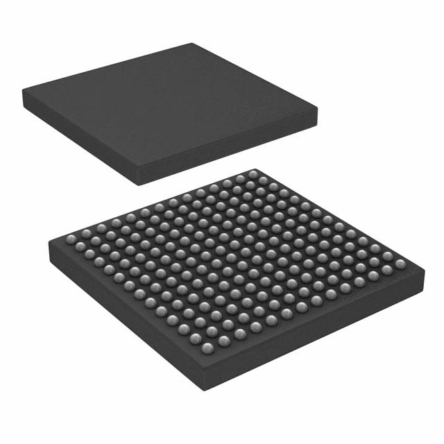
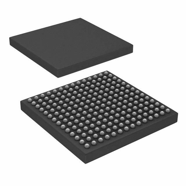
i960 Microprocessor IC i960 1 Core, 32-Bit 33MHz 196-BGA |
|---|---|
| Quantity | 461 Available (as of October 8, 2026) |
| Product Category | Microprocessors |
|---|---|
| Part Series | i960 |
| Manufacturer | Intel |
| Manufacturing Status | Obsolete |
| Manufacturer Standard Lead Time | Contact Us |
| Datasheet |
Specifications & Environmental
| Core Processor | i960 | Device Package | 196-BGA | ECCN | 3A991A2 | ||
|---|---|---|---|---|---|---|---|
| Grade | Commercial | Graphics Acceleration | No | HTS Code | 8542.31.0001 | ||
| Moisture Sensitivity Level | 4 (72 Hours) | Mounting Method | Surface Mount | Mounting Type | Surface Mount | ||
| Number of Cores/Bus Width | 1 Core, 32-Bit | Operating Temperature | 0°C ~ 100°C (TC) | Package / Case | 196-BGA | ||
| REACH Compliance | REACH Unknown | RoHS Compliance | RoHS non-compliant | Speed | 33MHz | ||
| Supplier Device Package | 196-BGA | Voltage – I/O | 3.3V |
Overview of GD80960JF33 – 32‑Bit i960 Microprocessor, 33 MHz, 196‑BGA
The GD80960JF33 is a single‑core, 32‑bit i960 microprocessor operating at 33 MHz in a 196‑ball BGA surface‑mount package. It implements the i960 embedded architecture with one‑instruction‑per‑clock execution and on‑chip resources to support compact, performance‑oriented embedded designs.
Designed for embedded applications, the GD80960JF33 combines instruction and data caches, on‑chip RAM and a rich interrupt/timer set to deliver deterministic performance, efficient memory utilization and simplified system integration at a 3.3 V supply level.
Key Features
- Core and Architecture Single 32‑bit i960 core with one‑instruction‑per‑clock execution and multiple register sets including sixteen 32‑bit global registers and sixteen 32‑bit local registers (8 sets).
- Clock and Performance 33 MHz operating speed; for the JA/JF/JS family variants the core clock operates at 1× the bus clock.
- Memory Subsystem Two‑way set‑associative instruction cache (4 KB for the JF variant), direct‑mapped data cache (2 KB for the JF/JD variants) and 1 KB on‑chip data RAM for critical variable storage and single‑cycle access.
- Interrupts and Timers High‑speed interrupt controller with programmable priorities (31 vectors in expanded mode), eight maskable pins plus NMI, and two on‑chip 32‑bit timers with prescaling options.
- Power and I/O 3.3 V supply voltage with 5 V tolerant inputs and TTL‑compatible outputs; includes a halt mode for low power operation.
- System and Test IEEE 1149.1 (JTAG) boundary‑scan compatibility for board‑level test and debug.
- Package and Mounting 196‑ball mini plastic BGA (MPBGA) surface‑mount package suitable for compact board layouts; commercial grade with an operating range of 0 °C to 100 °C.
- Memory Interface High‑bandwidth burst bus with 32‑bit multiplexed address/data lines and selectable 8/16/32‑bit bus widths for flexible memory configurations and support for unaligned accesses and both big‑ and little‑endian byte ordering.
Typical Applications
- Embedded Control Real‑time controllers and embedded appliances that benefit from deterministic one‑instruction‑per‑clock execution and on‑chip memory for tight control loops.
- Industrial Automation Machine control and sensor interfacing leveraging the device’s timers, interrupt controller and DRAM support for responsive I/O processing.
- Communications Equipment Control and management tasks in networking or telecom gear where cache, on‑chip RAM and configurable bus widths improve data handling and system integration.
- Instrumentation Measurement and test instruments that require a compact BGA package, JTAG boundary scan for testability, and operation across a commercial temperature range.
Unique Advantages
- Deterministic Execution: One‑instruction‑per‑clock architecture reduces instruction latency and simplifies performance planning for real‑time systems.
- Integrated Memory Resources: On‑chip instruction/data caches and 1 KB data RAM reduce external memory bandwidth needs and accelerate critical code paths.
- Flexible Memory Interface: Selectable bus widths (8/16/32‑bit) and a high‑bandwidth burst bus enable adaptable memory configurations for different system architectures.
- Robust Interrupt and Timer Support: Programmable interrupt priorities, maskable inputs and dual 32‑bit timers simplify responsive event handling and timing functions.
- 3.3 V I/O with 5 V Tolerance: Native 3.3 V operation with 5 V tolerant inputs and TTL‑compatible outputs eases integration with mixed‑voltage peripherals.
- Compact Surface‑Mount Packaging: 196‑ball BGA minimizes board area while providing a manufacturable surface‑mount solution for embedded applications.
- Standards‑Based Testability: IEEE 1149.1 JTAG boundary‑scan support improves board test and debugging capabilities during development and manufacturing.
- RoHS Compliant: Environmental compliance for regions and programs that require RoHS‑compatible components.
Why Choose GD80960JF33?
The GD80960JF33 positions a proven i960 embedded core in a compact 196‑BGA package, offering deterministic 33 MHz operation, integrated cache and on‑chip RAM, and comprehensive interrupt/timer resources. Its 3.3 V I/O with 5 V tolerant inputs and JTAG boundary‑scan capability make it suitable for embedded designs that require reliable performance, board testability and flexible memory interfaces.
This part is well suited for engineering teams building control, communications or instrumentation systems that need a balanced combination of integration, predictable execution and commercial‑grade operating range. The GD80960JF33 delivers a clear feature set for designs that prioritize deterministic behavior and simplified external memory usage.
Request a quote or submit an inquiry to obtain pricing, availability and lead‑time information for the GD80960JF33.





















Date Founded: 1968
Headquarters: Santa Clara, California, USA
Employees: 130,000+
Revenue: $54.23 Billion
Certifications and Memberships: ISO9001:2015, ISO14001:2015, ISO17025:2017, ISO27001:2022, ISO45001:2018, ISO50001:2018


