
SN74ACT8994FN
| Part Description |
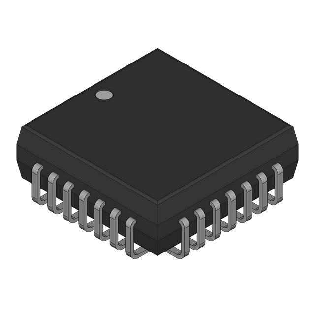
TI Digital Bus Monitor 16-Bit IEEE 1149.1 Boundary Scan PLCC |
|---|---|
| Quantity | 508 Available (as of October 8, 2026) |
| Product Category | Microprocessors |
|---|---|
| Part Series | SN74ACT |
| Manufacturer | Texas Instruments |
| Manufacturing Status | Active |
| Manufacturer Standard Lead Time | 1 Weeks |
| Datasheet |
Specifications & Environmental
| Device Package | 28-PLCC (11.51x11.51) | ECCN | EAR99 | Grade | Commercial | ||
|---|---|---|---|---|---|---|---|
| Graphics Acceleration | No | HTS Code | 8542.39.0001 | Moisture Sensitivity Level | 3 (168 Hours) | ||
| Mounting Method | Surface Mount | Number of Cores/Bus Width | 1 Core, 16-Bit | Operating Temperature | 0 °C – 70 °C (TA) | ||
| Package / Case | 28-LCC (J-Lead) | REACH Compliance | REACH Affected | RoHS Compliance | RoHS non-compliant | ||
| Speed | 50 MHz | Voltage – I/O | 5 V |
Overview of SN74ACT8994FN - TI Digital Bus Monitor 16-Bit IEEE 1149.1 Boundary Scan PLCC
The SN74ACT8994FN is a Digital Bus Monitor from Texas Instruments' SCOPE testability family, a boundary-scannable device that watches and records the state of a digital bus up to 16 bits wide. On-chip it holds a 1024-word by 16-bit scannable RAM, so captured bus activity can be stored and then shifted out through the IEEE 1149.1 test access port for analysis. Built in Advanced CMOS (ACT) and supplied in a PLCC, it turns a standard JTAG scan chain into a window onto live bus behavior.
Key Features
- 16-bit bus monitoring - samples and tracks the values present on a digital bus up to 16 bits wide.
- 1024 x 16 scannable RAM - an on-chip memory stores up to 1024 sixteen-bit bus states for later readout over the scan path.
- IEEE 1149.1 architecture - a standard JTAG test access port and boundary-scan structure let the monitor sit in an existing scan chain.
- SCOPE family member - works alongside other TI SCOPE testability devices for board-level test and debug.
- Advanced CMOS - the ACT process delivers low quiescent power with TTL-compatible logic levels.
- PLCC package - a surface-mount plastic leaded chip carrier (FN) for board-level integration.
Typical Applications
- Board-level test and debug - capturing bus traffic during development and manufacturing test without external logic analyzers.
- In-system fault diagnosis - reading back stored bus states through JTAG to localize faults.
- Scan-based instrumentation - adding observability to a bus inside a boundary-scan test strategy.
- Production test coverage - verifying bus behavior at end-of-line test alongside interconnect checks.
Unique Advantages
- Capture memory on chip - the 1024 x 16 RAM lets the device record a burst of bus activity rather than only snapshot a single state.
- Scan-path observability - monitoring through the 1149.1 port means no extra probe access is needed on a finished board.
- Fits existing test flows - as a SCOPE device it slots into the same infrastructure used for boundary-scan interconnect test.
- No external analyzer - recording bus activity into on-chip memory that reads out over JTAG can remove dedicated instrumentation from a design.
Why Choose SN74ACT8994FN?
The SN74ACT8994FN suits designs that want built-in visibility into a 16-bit bus through the JTAG chain, capturing activity into on-chip memory for readback instead of relying on external instruments. As a member of the TI SCOPE family, it integrates cleanly with boundary-scan test setups and remains a useful part for sustaining legacy test fixtures and boards that depend on it. The combination of a 16-bit monitored width and 1024-word capture depth lets it record a meaningful window of bus activity for later analysis.
Contact us for pricing, availability, and lead time on the SN74ACT8994FN, and tell us your test setup so we can help confirm fit.





















Date Founded: 1930
Headquarters: Dallas, Texas, USA
Employees: 34,000+
Revenue: $17.52 Billion
Certifications and Memberships: ISO9001:2015, ISO14001:2015, IATF16949:2016


