
10AX057N2F40I1HG
| Part Description |
Arria 10 GX Field Programmable Gate Array (FPGA) IC 588 42082304 570000 1517-BBGA, FCBGA |
|---|---|
| Quantity | 737 Available (as of June 15, 2026) |

| Product Category | Field Programmable Gate Array (FPGA) |
|---|---|
| Manufacturer | Intel |
| Manufacturing Status | Active |
| Manufacturer Standard Lead Time | 12 Weeks |
| Datasheet |
Specifications & Environmental
| Device Package | 1517-FBGA (40x40) | Grade | Industrial | Operating Temperature | -40°C – 100°C | ||
|---|---|---|---|---|---|---|---|
| Package / Case | 1517-BBGA, FCBGA | Number of I/O | 588 | Voltage | 870 mV - 980 mV | ||
| Mounting Method | Surface Mount | RoHS Compliance | RoHS Compliant | REACH Compliance | REACH Unaffected | ||
| Moisture Sensitivity Level | 3 (168 Hours) | Number of LABs/CLBs | 217080 | Number of Logic Elements/Cells | 570000 | ||
| Number of Gates | N/A | ECCN | 5A002A1 | HTS Code | 8542.39.0001 | ||
| Qualification | N/A | Total RAM Bits | 42082304 |
Overview of 10AX057N2F40I1HG – Arria 10 GX Field Programmable Gate Array
The 10AX057N2F40I1HG is an Intel Arria 10 GX FPGA in a 1517-BBGA (FCBGA) package, designed as a 20 nm mid-range, high-performance and power-efficient programmable logic device. It combines a large logic fabric and substantial embedded RAM with a broad set of I/O and transceiver features suited for wireless, wireline, broadcast, computing, medical, and defense applications.
Key value propositions include a high logic capacity (570,000 logic elements), extensive on-chip RAM (42,082,304 total bits), 588 I/O pins, industrial-grade temperature range, and a low-voltage core supply range—making it appropriate for complex, performance-sensitive designs.
Key Features
- Core Architecture Arria 10 GX device family implemented on a 20 nm process offering a balance of performance and power efficiency.
- Logic Capacity 570,000 logic elements to implement large-scale programmable logic and custom datapaths.
- Embedded Memory 42,082,304 total RAM bits of on-chip memory for buffering, LUT-based storage, and state retention.
- I/O and Connectivity 588 I/O pins to support wide external interface integration and system-level connectivity.
- Transceivers and IP Device family documentation highlights support for low-power serial transceivers and hard IP including PCIe Gen1/Gen2/Gen3 and enhanced PCS hard IP for Interlaken and 10 Gbps Ethernet.
- Power and Voltage Core voltage supply range from 870 mV to 980 mV allowing low-voltage system integration.
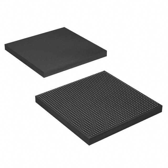
- Package and Mounting 1517-BBGA (supplier package: 1517-FBGA, 40×40) in a surface-mount form factor for PCB-level assembly.
- Operating Range and Compliance Industrial-grade operating temperature from −40 °C to 100 °C and RoHS compliant.
Typical Applications
- Wireless infrastructure — Channel and switch cards in remote radio heads and mobile backhaul systems where programmable logic and transceiver capabilities are required.
- Wireline networking — 40G/100G muxponders, transponders, and 100G line cards for packet processing, aggregation, and bridging tasks.
- Broadcast and professional media — Studio switches, transport servers, and videoconferencing or professional audio/video systems that need high-throughput I/O and programmable processing.
- Computing and storage acceleration — Flash cache, cloud computing servers, and server acceleration functions that leverage large logic and on-chip memory.
- Medical and defense systems — Diagnostic imaging, radar, and electronic warfare applications that benefit from programmable compute, deterministic latency, and industrial temperature support.
Unique Advantages
- High programmable capacity: 570,000 logic elements enable complex algorithm and datapath implementation without external logic expansion.
- Large on-chip memory: 42,082,304 RAM bits reduce dependence on external memory for many buffering and stateful tasks, simplifying board-level design.
- Rich I/O footprint: 588 I/Os provide flexibility for interfacing with multiple high-speed peripherals and wide external buses.
- Industrial thermal range: −40 °C to 100 °C rating supports deployment in harsh or temperature-variable environments.
- Compact, surface-mount package: 1517-BBGA (40×40 FCBGA) delivers high-density integration for space-constrained PCBs.
- Family-level IP and transceiver support: Built-in hard IP options (PCIe Gen1–Gen3, enhanced PCS for Interlaken and 10 Gbps Ethernet) and low-power serial transceivers streamline common high-speed interface implementations.
Why Choose 10AX057N2F40I1HG?
The 10AX057N2F40I1HG Arria 10 GX FPGA offers a balanced combination of large logic capacity, significant embedded memory, and extensive I/O in an industrial-grade, surface-mount BBGA package. Its 20 nm architecture and supported hard IP features make it suitable for mid-range applications that require both performance and power efficiency.
This device is appropriate for engineering teams building wireless and wireline infrastructure, broadcast systems, compute/storage accelerators, medical imaging, and defense electronics that need scalable programmable logic with documented family-level IP and transceiver capabilities. The Arria 10 device documentation provides design guidance and device-handbook resources to support development and deployment.
Request a quote or submit an inquiry for pricing and availability for part number 10AX057N2F40I1HG. Our team can provide lead-time and procurement details to support your design schedule.


Date Founded: 1968
Headquarters: Santa Clara, California, USA
Employees: 130,000+
Revenue: $54.23 Billion
Certifications and Memberships: ISO9001:2015, ISO14001:2015, ISO17025:2017, ISO27001:2022, ISO45001:2018, ISO50001:2018


