
10AX057N3F40I2LG
| Part Description |
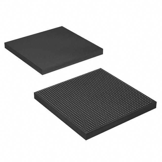
Arria 10 GX Field Programmable Gate Array (FPGA) IC 588 42082304 570000 1517-BBGA, FCBGA |
|---|---|
| Quantity | 754 Available (as of June 15, 2026) |

| Product Category | Field Programmable Gate Array (FPGA) |
|---|---|
| Manufacturer | Intel |
| Manufacturing Status | Active |
| Manufacturer Standard Lead Time | 12 Weeks |
| Datasheet |
Specifications & Environmental
| Device Package | 1517-FCBGA (40x40) | Grade | Industrial | Operating Temperature | -40°C – 100°C | ||
|---|---|---|---|---|---|---|---|
| Package / Case | 1517-BBGA, FCBGA | Number of I/O | 588 | Voltage | 870 mV - 930 mV | ||
| Mounting Method | Surface Mount | RoHS Compliance | RoHS Compliant | REACH Compliance | REACH Unaffected | ||
| Moisture Sensitivity Level | 3 (168 Hours) | Number of LABs/CLBs | 217080 | Number of Logic Elements/Cells | 570000 | ||
| Number of Gates | N/A | ECCN | 3A001A7B | HTS Code | 8542.39.0001 | ||
| Qualification | N/A | Total RAM Bits | 42082304 |
Overview of 10AX057N3F40I2LG – Arria 10 GX FPGA (1517-FCBGA)
The Intel Arria 10 GX Field Programmable Gate Array (10AX057N3F40I2LG) is a 20 nm mid-range FPGA device providing a balance of high performance and power efficiency. It delivers substantial logic capacity, embedded memory, and I/O capability in a 1517-FCBGA (40×40) surface-mount package.
Designed for midrange, power-sensitive applications across wireless, wireline, broadcast, computing and storage, medical, and military markets, the device emphasizes performance, configurable logic, and integrated hard IP to accelerate system-level designs.
Key Features
- Device family & process – Part of the Intel Arria 10 family of 20 nm mid-range FPGAs and SoCs, engineered for improved performance and power efficiency relative to prior generations.
- Logic capacity – 570,000 logic elements (cells) to implement large, complex designs.
- Embedded memory – 42,082,304 total RAM bits across the device, supported by configurable embedded memory blocks and multiple memory configuration options.
- I/O and transceivers – 588 device I/O pins and low-power serial transceiver technology, with PMA and PCS features and multiple transceiver channel options for high-speed serial links.
- Hard IP – Includes PCIe Gen1/Gen2/Gen3 hard IP and enhanced PCS hard IP for Interlaken and 10 Gbps Ethernet as documented for the Arria 10 family.
- DSP capabilities – Variable-precision DSP blocks for signal processing and compute-intensive functions.
- Clocking & PLLs – Comprehensive clock networks with fractional synthesis and I/O PLLs for flexible clocking and timing architectures.
- SoC options – Family documentation includes support for SoC devices with a Hard Processor System (HPS), enabling tighter CPU–FPGA integration where required.
- Power and thermal – Voltage supply range of 870 mV to 930 mV and an operating temperature range of −40 °C to 100 °C suitable for industrial-grade deployments.
- Package & mounting – 1517-BBGA / 1517-FCBGA (40×40) surface-mount package; RoHS compliant.
Typical Applications
- Wireless infrastructure – Channel and switch cards in remote radio heads and mobile backhaul equipment, where programmable logic and high-speed I/O enable protocol handling and data aggregation.
- Wireline networking – 40G/100G muxponders, transponders, and line cards for bridging and aggregation using the device's transceivers and protocol hard IP.
- Broadcast and professional AV – Studio switches and transport systems that benefit from high-capacity logic, low-latency processing, and flexible I/O.
- Computing and storage – Server acceleration, flash cache, and cloud infrastructure tasks that leverage embedded memory, DSP blocks, and PCIe hard IP.
- Defense and specialized systems – Radar, electronic warfare, and secure communications applications that require configurable logic density and industrial operating range.
Unique Advantages
- High programmable capacity: 570,000 logic elements enable implementation of large-scale logic, control, and datapath functions on a single device, reducing system complexity.
- Extensive embedded memory: Over 42 million RAM bits provide on-chip storage for buffers, caches, and data structures, minimizing external memory dependence.
- Broad hard IP support: Integrated PCIe Gen1/Gen2/Gen3 and enhanced PCS blocks for Interlaken and 10 Gbps Ethernet accelerate time to market for common high-speed interfaces.
- Flexible high-speed I/O: 588 I/O pins combined with low-power serial transceivers and comprehensive clocking resources support varied I/O and link requirements.
- Industrial-ready thermal range: Rated for −40 °C to 100 °C operation and manufactured in a surface-mount 1517-FCBGA package suited to industrial applications.
- Power-conscious architecture: Family-level power-saving technologies and a narrow supply-voltage window (870 mV–930 mV) support designs with strict power budgets.
Why Choose 10AX057N3F40I2LG?
The 10AX057N3F40I2LG Arria 10 GX device offers a compelling mix of logic density, embedded memory, high-speed I/O, and hardened protocol IP for midrange systems that need configurable performance with power-conscious operation. Its industrial operating range and package options make it suitable for demanding deployments across communications, broadcast, compute, and defense segments.
For engineers and procurement teams, this device delivers a scalable FPGA platform within the Arria 10 family, supported by a set of architectural features—DSP blocks, PLL/clocking networks, transceivers, and hard IP—that reduce board-level complexity and accelerate development.
Request a quote or submit an RFQ today to receive pricing, availability, and lead-time information for 10AX057N3F40I2LG.


Date Founded: 1968
Headquarters: Santa Clara, California, USA
Employees: 130,000+
Revenue: $54.23 Billion
Certifications and Memberships: ISO9001:2015, ISO14001:2015, ISO17025:2017, ISO27001:2022, ISO45001:2018, ISO50001:2018


