
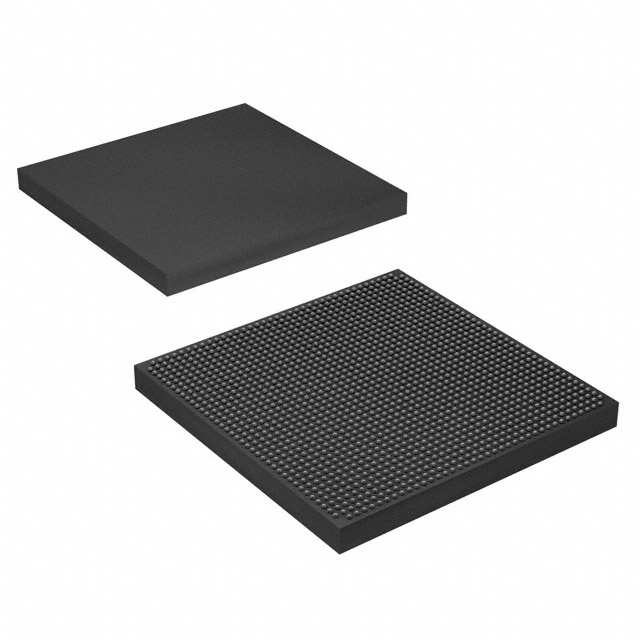
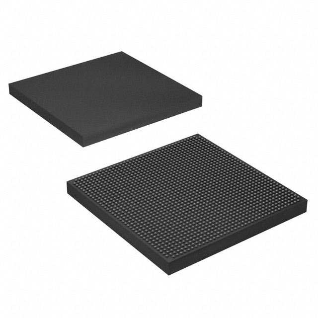
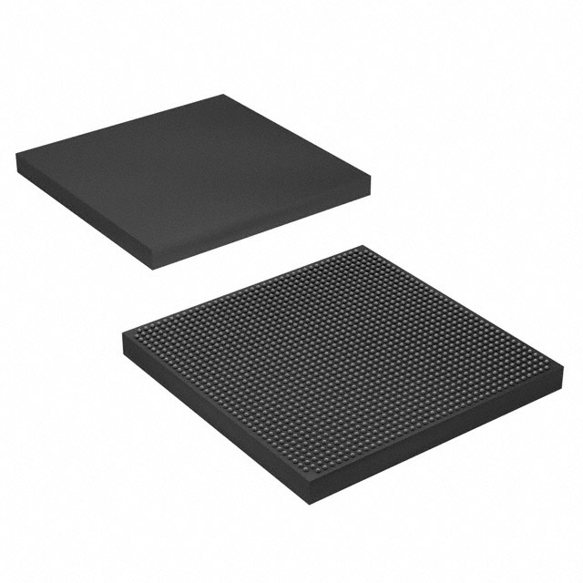
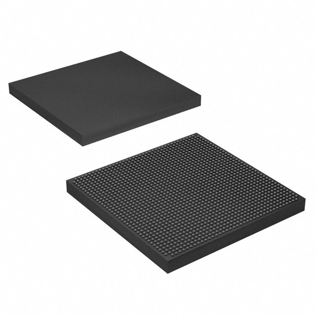
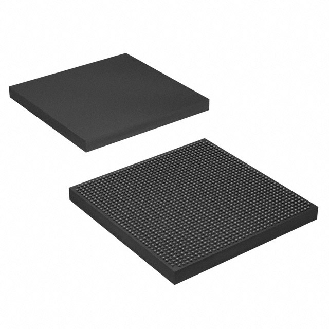
10AX115H2F34E2SG
| Part Description |
Arria 10 GX Field Programmable Gate Array (FPGA) IC 504 68857856 1150000 1152-BBGA, FCBGA |
|---|---|
| Quantity | 805 Available (as of October 7, 2026) |
| Product Category | Field Programmable Gate Array (FPGA) |
|---|---|
| Manufacturer | Intel |
| Manufacturing Status | Active |
| Manufacturer Standard Lead Time | 16 Weeks |
| Datasheet |
Specifications & Environmental
| Device Package | 1152-FCBGA (35x35) | Grade | Extended | Operating Temperature | 0°C – 100°C | ||
|---|---|---|---|---|---|---|---|
| Package / Case | 1152-BBGA, FCBGA | Number of I/O | 504 | Voltage | 870 mV - 980 mV | ||
| Mounting Method | Surface Mount | RoHS Compliance | RoHS Compliant | REACH Compliance | REACH Unaffected | ||
| Moisture Sensitivity Level | 3 (168 Hours) | Number of LABs/CLBs | 427200 | Number of Logic Elements/Cells | 1150000 | ||
| Number of Gates | N/A | ECCN | 3A001A7A | HTS Code | 8542.39.0001 | ||
| Qualification | N/A | Total RAM Bits | 68857856 |
Overview of 10AX115H2F34E2SG – Arria 10 GX FPGA, 1152-FCBGA
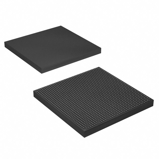
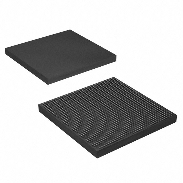
The 10AX115H2F34E2SG is an Intel Arria 10 GX Field Programmable Gate Array (FPGA) in a 1152-FCBGA (35×35) package. It is part of the Arria 10 device family of 20 nm mid-range FPGAs designed for high-performance, power-efficient designs.
Built for midrange applications across wireless, wireline, broadcast, computing, storage, medical, and defense markets, this device delivers large programmable logic capacity and dense embedded memory alongside integrated I/O and transceiver support to accelerate system-level designs.
Key Features
- Core Capacity — 1,150,000 logic elements to implement complex, high-density logic and custom datapaths.
- Embedded Memory — 68,857,856 total RAM bits for on-chip buffering, large FIFOs, and memory-rich accelerators.
- I/O Density — 504 I/O pins to support broad external interfacing and multi-channel connectivity.
- Transceivers and Interfaces — Family-level support for low-power serial transceivers, enhanced PCS hard IP for 10 Gbps Ethernet and Interlaken, and PCIe Gen1/Gen2/Gen3 hard IP as documented for Arria 10 devices.
- DSP and Signal Processing — Variable-precision DSP block architecture (Arria 10 family) suitable for multiply-accumulate and signal-processing tasks.
- Clocking and PLLs — Comprehensive clock networks with fractional synthesis and I/O PLL sources as part of the Arria 10 device architecture.
- Power and Voltage — Supported supply voltage range of 870 mV to 980 mV, reflecting the device’s power-optimized 20 nm implementation.
- Package and Mounting — 1152-BBGA (1152-FCBGA, 35×35) surface-mount package suitable for high-density PCB integration.
- Operating Range and Grade — Extended grade with an operating temperature range of 0 °C to 100 °C and RoHS compliance.
Typical Applications
- Wireless Infrastructure — Channel and switch cards, remote radio heads, and mobile backhaul systems that require programmable logic and high-bandwidth interfacing.
- Wireline and Optical Networking — 40G/100G muxponders, transponders, and line cards using embedded memory and transceiver IP for packet aggregation and transport functions.
- Compute and Storage Acceleration — Flash cache, server acceleration, and cloud compute offload where large logic capacity and on-chip RAM accelerate data-path processing.
- Broadcast and Professional AV — Studio switches, videoconferencing and transport systems that need flexible I/O mapping and deterministic processing.
Unique Advantages
- Large Programmable Fabric: 1,150,000 logic elements enable implementation of complex control logic, large state machines, and parallel datapaths without immediate external ASIC development.
- Significant On-Chip Memory: Nearly 69 Mbit of embedded RAM supports deep buffering, wide FIFOs, and memory-intensive algorithms directly on the FPGA die.
- High I/O Count: 504 I/O pins provide flexibility to interface multiple external devices, memories, and high-speed front-ends from a single device.
- Integrated Interface IP (Family-Level): Arria 10 device documentation includes support for PCIe Gen1/2/3 and advanced PCS/IP blocks, simplifying integration of high-speed links.
- Power-Optimized Operation: Narrow supply voltage range (870–980 mV) and 20 nm technology deliver a power-aware platform for energy-sensitive midrange designs.
- Production-Ready Package and Grade: 1152-FCBGA surface-mount package and Extended-grade operating range (0 °C to 100 °C) support deployment in demanding commercial and industrial environments.
Why Choose 10AX115H2F34E2SG?
The 10AX115H2F34E2SG positions itself as a high-capacity, power-efficient midrange FPGA within the Intel Arria 10 family. Its combination of 1,150,000 logic elements, large embedded RAM, high I/O count, and family-level support for advanced transceiver and interface IP makes it suitable for designs that require substantial on-chip resources and flexible connectivity without moving to a custom ASIC.
Engineers and system designers targeting wireless infrastructure, networking, storage acceleration, and professional AV applications will find the device’s integration and device-family documentation helpful for accelerating development, scaling designs, and maintaining long-term product support.
If you would like a quote or have questions about using the 10AX115H2F34E2SG in your design, submit a request or inquiry and our team will respond with pricing and availability information.





















Date Founded: 1968
Headquarters: Santa Clara, California, USA
Employees: 130,000+
Revenue: $54.23 Billion
Certifications and Memberships: ISO9001:2015, ISO14001:2015, ISO17025:2017, ISO27001:2022, ISO45001:2018, ISO50001:2018


