
10AX115H2F34I2SG
| Part Description |
Arria 10 GX Field Programmable Gate Array (FPGA) IC 504 68857856 1150000 1152-BBGA, FCBGA |
|---|---|
| Quantity | 991 Available (as of June 10, 2026) |

| Product Category | Field Programmable Gate Array (FPGA) |
|---|---|
| Manufacturer | Intel |
| Manufacturing Status | Active |
| Manufacturer Standard Lead Time | 16 Weeks |
| Datasheet |
Specifications & Environmental
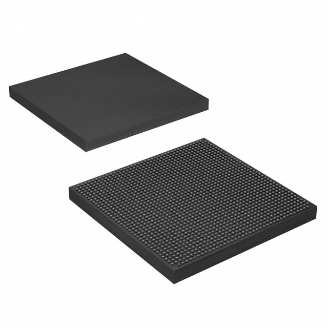
| Device Package | 1152-FCBGA (35x35) | Grade | Industrial | Operating Temperature | -40°C – 100°C | ||
|---|---|---|---|---|---|---|---|
| Package / Case | 1152-BBGA, FCBGA | Number of I/O | 504 | Voltage | 870 mV - 980 mV | ||
| Mounting Method | Surface Mount | RoHS Compliance | RoHS Compliant | REACH Compliance | REACH Unaffected | ||
| Moisture Sensitivity Level | 3 (168 Hours) | Number of LABs/CLBs | 427200 | Number of Logic Elements/Cells | 1150000 | ||
| Number of Gates | N/A | ECCN | 3A001A7A | HTS Code | 8542.39.0001 | ||
| Qualification | N/A | Total RAM Bits | 68857856 |
Overview of 10AX115H2F34I2SG – Arria 10 GX Field Programmable Gate Array (FPGA)
The 10AX115H2F34I2SG is an Intel Arria 10 GX field programmable gate array (FPGA) in a 1152-FCBGA package. It is a 20‑nm, mid-range FPGA designed for high-performance, power‑sensitive applications across communications, broadcast, computing, medical, and defense markets.
This device combines a large logic fabric with substantial on‑chip memory, high-speed I/O, and integrated protocol IP to support complex system designs that require high logic density, flexible interfacing, and industrial temperature operation.
Key Features
- Logic Capacity — 1,150,000 logic elements to implement large digital designs and complex custom logic functions.
- On‑Chip Memory — 68,857,856 total RAM bits for buffering, caching, and embedded data storage within FPGA fabric.
- I/O and Package — 504 user I/O pins in a 1152‑FBGA (35×35) package, enabling dense board-level connectivity and signal routing.
- Industrial Temperature Grade — Rated for operation from −40 °C to 100 °C to meet robust environmental requirements.
- Supply Voltage Range — Core operating range of 870 mV to 980 mV to match system power architectures and regulators.
- High‑Speed Interfaces and IP — Includes support for PCIe Gen1/Gen2/Gen3 hard IP, enhanced PCS hard IP for Interlaken and 10 Gbps Ethernet, and low‑power serial transceivers as described in the device overview.
- DSP and Clocking — Variable‑precision DSP blocks and a flexible clock network with PLL clock sources for high‑throughput signal processing and timing control.
- Configuration and Reliability — Features described in the device overview include dynamic and partial reconfiguration options and SEU error detection and correction mechanisms.
Typical Applications
- Wireless Infrastructure — Channel and switch cards in remote radio heads and mobile backhaul equipment that benefit from high logic density and integrated transceivers.
- Wireline and Optical Networking — 40G/100G muxponders, transponders, and line cards leveraging PCIe and high-speed serial support for packet and transport processing.
- Computing and Storage — Flash cache, server acceleration, and cloud infrastructure components needing large on‑chip memory and flexible custom logic.
- Broadcast and Media — Studio switches, videoconferencing, and professional audio/video systems requiring low-latency processing and dense I/O.
- Medical and Defense Systems — Diagnostic imaging and radar/electronic warfare applications that require high performance under industrial temperature ranges.
Unique Advantages
- High Logic Density: 1,150,000 logic elements provide the capacity to implement large-scale digital designs without external glue logic.
- Substantial Embedded Memory: Nearly 69 million bits of on‑chip RAM reduce dependence on external memory for buffering and data paths.
- Comprehensive High‑Speed Connectivity: Integrated hard IP for PCIe and 10 Gbps Ethernet plus low‑power serial transceivers simplify high‑bandwidth system design.
- Robust Industrial Operation: −40 °C to 100 °C rating supports deployment in demanding thermal environments.
- Compact, High‑Pin Package: 1152‑FCBGA (35×35) package with 504 I/Os enables dense board integration and extensive peripheral interfacing.
- Flexible Power and Clocking: Core voltage range of 870–980 mV and programmable PLLs support optimized power delivery and tailored clock architectures.
Why Choose 10AX115H2F34I2SG?
The 10AX115H2F34I2SG positions itself as a high‑capacity, mid‑range FPGA suited for power‑sensitive, performance‑driven systems. With over one million logic elements, large on‑chip memory, industrial temperature support, and integrated high‑speed protocol IP, it is tailored for designers building complex communications, computing, and signal processing applications.
Choose this device when you need a scalable, integrated FPGA platform that balances logic density, embedded memory, and robust I/O in a compact FCBGA package—backed by the Arria 10 device family architecture and configuration options described in the device overview.
Request a quote or submit an inquiry to receive pricing, availability, and technical support for the 10AX115H2F34I2SG.


Date Founded: 1968
Headquarters: Santa Clara, California, USA
Employees: 130,000+
Revenue: $54.23 Billion
Certifications and Memberships: ISO9001:2015, ISO14001:2015, ISO17025:2017, ISO27001:2022, ISO45001:2018, ISO50001:2018


