
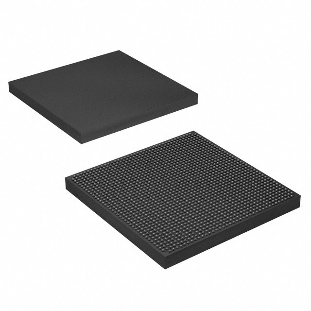
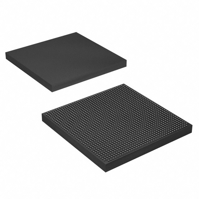
10AX115H3F34E2LG
| Part Description |
Arria 10 GX Field Programmable Gate Array (FPGA) IC 504 68857856 1150000 1152-BBGA, FCBGA |
|---|---|
| Quantity | 201 Available (as of October 7, 2026) |
| Product Category | Field Programmable Gate Array (FPGA) |
|---|---|
| Manufacturer | Intel |
| Manufacturing Status | Active |
| Manufacturer Standard Lead Time | 16 Weeks |
| Datasheet |
Specifications & Environmental
| Device Package | 1152-FCBGA (35x35) | Grade | Extended | Operating Temperature | 0°C – 100°C | ||
|---|---|---|---|---|---|---|---|
| Package / Case | 1152-BBGA, FCBGA | Number of I/O | 504 | Voltage | 870 mV - 930 mV | ||
| Mounting Method | Surface Mount | RoHS Compliance | RoHS Compliant | REACH Compliance | REACH Unaffected | ||
| Moisture Sensitivity Level | 3 (168 Hours) | Number of LABs/CLBs | 427200 | Number of Logic Elements/Cells | 1150000 | ||
| Number of Gates | N/A | ECCN | 3A001A7A | HTS Code | 8542.39.0001 | ||
| Qualification | N/A | Total RAM Bits | 68857856 |
Overview of 10AX115H3F34E2LG – Arria 10 GX FPGA, 1152‑FCBGA
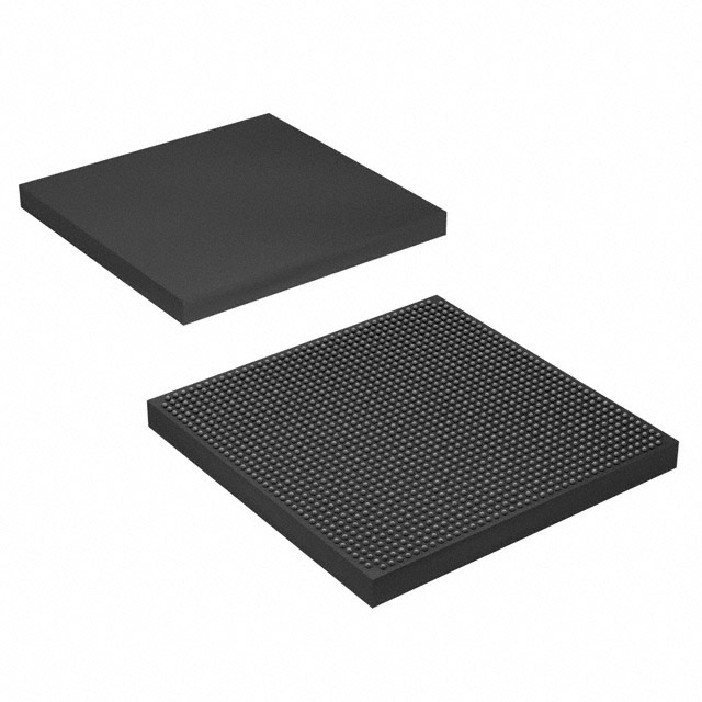
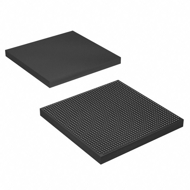
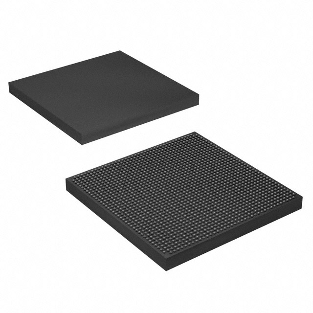
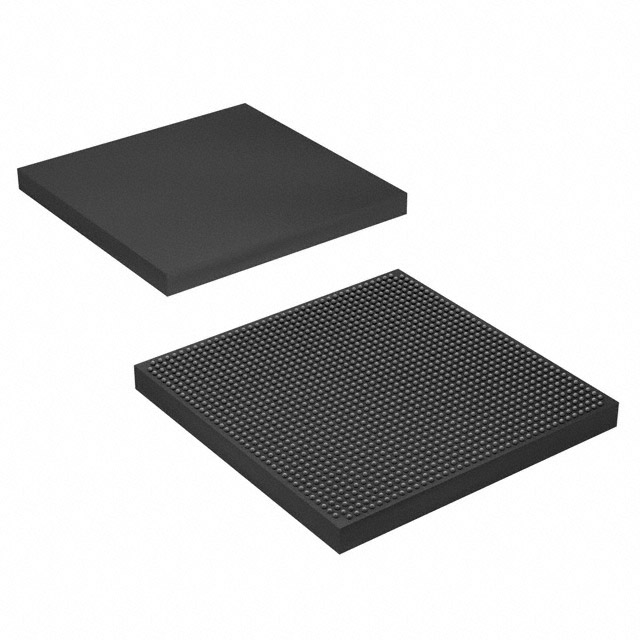
The 10AX115H3F34E2LG is an Intel Arria 10 GX field‑programmable gate array (FPGA) in a 1152‑ball FCBGA package designed for mid‑range, high‑performance applications. It combines a high logic element count and large on‑chip memory with low‑power 20‑nm device architecture to address demanding use cases across wireless, wireline, broadcast, computing, medical and defense markets.
This surface‑mount, extended‑grade device supports a wide operating range and integration features useful for system designers seeking performance, flexible I/O and embedded IP options in a compact 35×35 mm package.
Key Features
- High logic capacity — 1,150,000 logic elements (cells) to implement complex custom logic and acceleration functions.
- Large embedded memory — 68,857,856 total RAM bits for on‑chip buffering, caches, and data path storage.
- Rich I/O resources — 504 I/O pins to support multiple interfaces and high pin‑count system connections.
- Advanced transceiver and IP support — Arria 10 family features include low‑power serial transceivers and hard IP blocks for protocols such as PCIe and high‑speed Ethernet (as described in the device overview).
- Flexible clocking and PLLs — Comprehensive clock network architecture with fractional synthesis and I/O PLLs for precise timing and multi‑clock domain designs.
- Power and process — 20‑nm device architecture optimized for performance and power efficiency; voltage supply range 870 mV to 930 mV.
- Package and mounting — 1152‑FBGA (1152‑FCBGA, 35×35 mm) supplier device package; surface‑mount assembly.
- Extended temperature grade — Rated for 0 °C to 100 °C operation for applications requiring wider commercial temperature range.
- Standards and compliance — RoHS compliant.
Typical Applications
- Wireless infrastructure — Channel and switch cards in remote radio heads and mobile backhaul systems that need high logic density and embedded memory for signal processing.
- Wireline networking — 40G/100G muxponder and transponder line cards and aggregation systems leveraging high I/O and transceiver capabilities.
- Broadcast and video — Studio switching and professional audio/video processing where large memory and programmable logic facilitate real‑time media handling.
- Computing and storage — Server acceleration, flash cache and cloud computing servers benefitting from dense logic and on‑chip RAM for offload and low‑latency processing.
- Medical imaging and diagnostics — Diagnostic scanners and imaging equipment that require customizable processing pipelines and substantial on‑chip memory.
Unique Advantages
- High integration in a compact package: 1,150,000 logic elements and 68,857,856 RAM bits in a 35×35 mm 1152‑FCBGA enable dense integration while keeping PCB footprint small.
- Designed for performance and power efficiency: 20‑nm Arria 10 architecture delivers a balance of performance and power savings described in the device overview.
- Flexible system interfacing: 504 I/O pins paired with transceiver and PLL features support diverse protocol implementations and multi‑interface designs.
- Extended commercial temperature range: 0 °C to 100 °C rating suits designs that require wider operating conditions than standard commercial parts.
- Embedded IP and ecosystem documentation: The Arria 10 device family includes hard IP blocks (PCIe, Ethernet, etc.) and device handbooks to streamline design integration and verification.
Why Choose 10AX115H3F34E2LG?
The 10AX115H3F34E2LG Arria 10 GX FPGA positions itself as a high‑capacity, energy‑efficient programmable platform for mid‑range applications that demand substantial logic, large on‑chip memory, and flexible I/O. Its extended‑grade rating and robust package options make it suitable for varied commercial and professional systems requiring reliable, scalable FPGA resources.
Designers looking to implement complex signal processing, network aggregation, media handling or server acceleration can leverage this device’s logic density, embedded memory and supported IP blocks to reduce system complexity and accelerate time‑to‑market while using the Arria 10 documentation and ecosystem for development and validation.
Request a quote or submit an inquiry for 10AX115H3F34E2LG to get pricing and availability information.





















Date Founded: 1968
Headquarters: Santa Clara, California, USA
Employees: 130,000+
Revenue: $54.23 Billion
Certifications and Memberships: ISO9001:2015, ISO14001:2015, ISO17025:2017, ISO27001:2022, ISO45001:2018, ISO50001:2018


