
5962-9958602QYC
| Part Description |
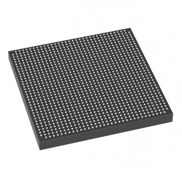
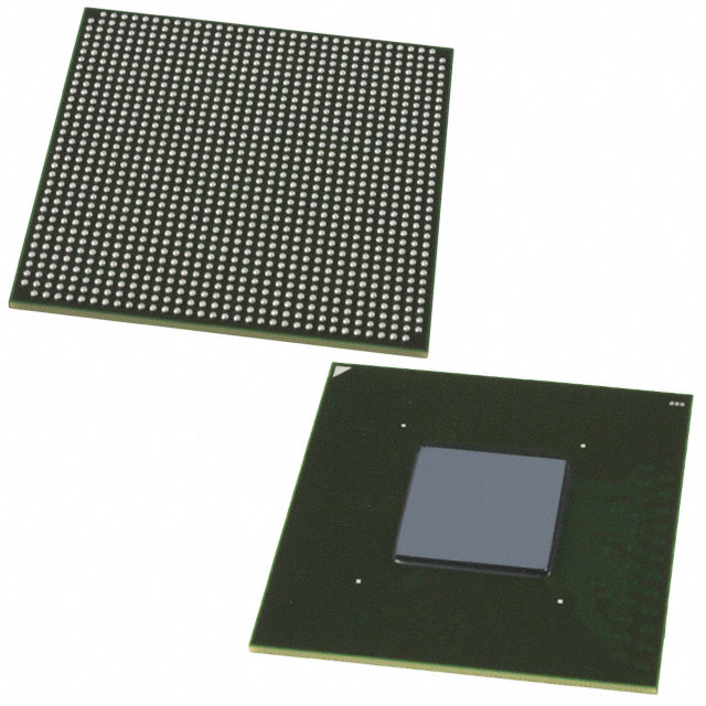
SX Field Programmable Gate Array (FPGA) IC 174 208-BFCQFP with Tie Bar |
|---|---|
| Quantity | 816 Available (as of June 18, 2026) |

| Product Category | Field Programmable Gate Array (FPGA) |
|---|---|
| Manufacturer | Microchip Technology |
| Manufacturing Status | Active |
| Manufacturer Standard Lead Time | 60 Weeks |
| Datasheet |
Specifications & Environmental
| Device Package | 208-CQFP (75x75) | Grade | Military | Operating Temperature | -55°C – 125°C | ||
|---|---|---|---|---|---|---|---|
| Package / Case | 208-BFCQFP with Tie Bar | Number of I/O | 174 | Voltage | 3 V - 5.5 V | ||
| Mounting Method | Surface Mount | RoHS Compliance | RoHS non-compliant | REACH Compliance | REACH Unaffected | ||
| Moisture Sensitivity Level | 3 (168 Hours) | Number of LABs/CLBs | 2880 | Number of Logic Elements/Cells | 2880 | ||
| Number of Gates | 48000 | ECCN | 3A001A2C | HTS Code | 8542.39.0001 | ||
| Qualification | N/A |
Overview of 5962-9958602QYC – SX Field Programmable Gate Array (FPGA) IC, 174 I/Os, 208-BFCQFP
The 5962-9958602QYC is a military-grade SX family Field Programmable Gate Array (FPGA) from Microchip Technology supplied in a 208-pin BFCQFP package with tie bar. It delivers a high I/O count and a substantial logic capacity for embedded designs that require nonvolatile, single-chip programmable logic with rugged environmental capability.
Designed for applications that demand wide voltage tolerance and extended temperature operation, this device provides flexible I/O support and secure configuration features drawn from the SX-A family architecture.
Key Features
- Logic Capacity — 2,880 logic elements (cells) and approximately 48,000 system gates provide programmable logic resources for complex glue logic and control functions.
- I/O Count & Flexibility — 174 user I/O pins enable broad external interfacing. Series-level I/O support includes configurable options for 3.3 V / 5 V PCI, 5 V TTL, 3.3 V LVTTL and 2.5 V LVCMOS2 signaling, and 5 V input tolerance with 5 V drive strength.
- Nonvolatile Single-Chip Architecture — SX family nonvolatile configuration avoids the need for external configuration memory, simplifying BOM and startup behavior.
- Voltage & Power — Operates from 3 V to 5.5 V, supporting mixed-voltage designs and legacy 5 V systems.
- Thermal & Grade — Military grade with an operating temperature range of −55 °C to +125 °C for deployment in harsh environments.
- Package & Mounting — Surface-mount 208-BFCQFP with tie bar; supplier device package listed as 208-CQFP (75×75).
- SRAM/Memory — Total RAM bits: 0, for deterministic, register-based logic implementation.
- System & Debug Support — Series features include boundary-scan (IEEE 1149.1/JTAG) for board-level test and in-system diagnostic capabilities.
- Security & Reliability — Series-level secure programming technology (FuseLock™) protects designs against reverse engineering and unauthorized readback.
- Standards & Performance — SX family datasheet lists up to 250 MHz system performance and support for 66 MHz PCI operation as part of the architecture's performance profile.
- Regulatory — RoHS compliant.
Typical Applications
- Military and Aerospace Systems — Military-grade temperature range and packaging make this FPGA suitable for control and interface logic in ruggedized electronic assemblies.
- Legacy 5 V System Integration — Configurable 5 V-tolerant I/Os and mixed-voltage operation simplify interfacing with older TTL and PCI-based subsystems.
- High-Reliability Embedded Control — Nonvolatile single-chip configuration and JTAG boundary-scan support reliable boot and in-system test for mission-critical embedded controllers.
- Communications and Interface Logic — High I/O count supports protocol translation, bus bridging, and glue logic in communications line cards and backplane interfaces.
Unique Advantages
- Wide Operating Range: Military-grade temperature rating (−55 °C to +125 °C) and 3 V–5.5 V supply allow deployment in extreme environments and mixed-voltage systems.
- High I/O Density: 174 user I/Os enable complex external interconnects without additional multiplexing or expansion logic.
- Deterministic, Nonvolatile Configuration: Single-chip nonvolatile architecture removes the need for external configuration memory and improves system reliability at power-up.
- Security Built-In: Series FuseLock™ secure programming reduces the risk of IP exposure and design cloning.
- Testability and Diagnostics: IEEE 1149.1 (JTAG) boundary-scan and series in-system diagnostic features simplify board-level test and field diagnostics.
- RoHS Compliant and Surface-Mount Ready: Meets environmental compliance requirements and ships in a 208-pin surface-mount package for standard assembly processes.
Why Choose 5962-9958602QYC?
This FPGA combines a robust logic resource set (2,880 logic elements, ~48,000 gates) with a high I/O count and a military-grade thermal envelope, making it well suited for applications that demand reliability, deterministic behavior and flexible voltage-domain interfacing. The nonvolatile, single-chip SX architecture reduces external components and streamlines board-level design.
Designers targeting rugged embedded systems, legacy 5 V interfacing, and applications requiring secure configuration and in-system test capability will find the 5962-9958602QYC a pragmatic choice for reducing BOM complexity while meeting demanding environmental requirements.
Request a quote or submit a parts inquiry for pricing and availability of 5962-9958602QYC to evaluate suitability for your next high-reliability FPGA design.


Date Founded: 1989
Headquarters: Chandler, Arizona, USA
Employees: 22,000+
Revenue: $8.349 Billion
Certifications and Memberships: ISO9001:2015, IATF16949:2016, AS 9100D


