
5962-9958601QYC
| Part Description |
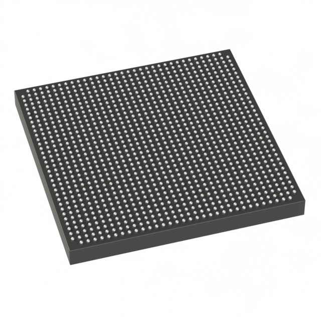
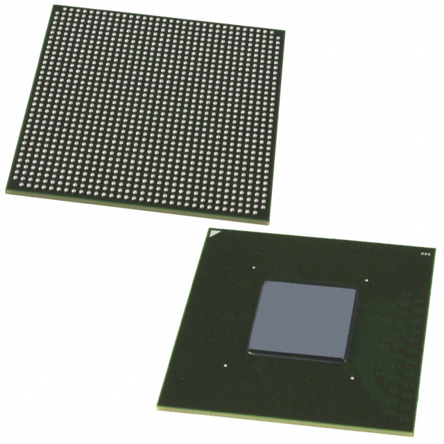
SX Field Programmable Gate Array (FPGA) IC 174 208-BFCQFP with Tie Bar |
|---|---|
| Quantity | 74 Available (as of June 18, 2026) |

| Product Category | Field Programmable Gate Array (FPGA) |
|---|---|
| Manufacturer | Microchip Technology |
| Manufacturing Status | Active |
| Manufacturer Standard Lead Time | 60 Weeks |
| Datasheet |
Specifications & Environmental
| Device Package | 208-CQFP (75x75) | Grade | Military | Operating Temperature | -55°C – 125°C | ||
|---|---|---|---|---|---|---|---|
| Package / Case | 208-BFCQFP with Tie Bar | Number of I/O | 174 | Voltage | 3 V - 5.5 V | ||
| Mounting Method | Surface Mount | RoHS Compliance | RoHS non-compliant | REACH Compliance | REACH Unaffected | ||
| Moisture Sensitivity Level | 3 (168 Hours) | Number of LABs/CLBs | 2880 | Number of Logic Elements/Cells | 2880 | ||
| Number of Gates | 48000 | ECCN | 3A001A2C | HTS Code | 8542.39.0001 | ||
| Qualification | N/A |
Overview of 5962-9958601QYC – SX FPGA, 174 I/O, 208-BFCQFP (Tie Bar), Military Grade
The 5962-9958601QYC is a Microchip Technology SX family field programmable gate array supplied in a 208‑pin BFCQFP package with tie bar. It delivers a mid‑range FPGA capacity with 48,000 system gates and 2,880 logic elements, targeting applications that require high I/O density, deterministic timing and military temperature performance.
Built for mixed‑voltage systems and rugged environments, this FPGA combines configurable I/O flexibility, nonvolatile single‑chip configuration, and a broad operating range to support embedded, PCI and military-class designs.
Key Features
- Logic Capacity — 48,000 system gates and 2,880 logic elements provide substantial programmable logic resources for mid‑complexity designs.
- I/O Density — 174 user‑programmable I/O pins give high pin count in a 208‑pin package for dense board-level integration.
- Performance — SX family documented performance up to 250 MHz system and 350 MHz internal operation supports demanding timing requirements.
- Mixed‑Voltage Support — Configurable I/O support and 2.5 V, 3.3 V and 5 V mixed‑voltage operation with 5 V input tolerance and 5 V drive strength enable direct interfacing to a variety of logic standards.
- Power and Reliability — Power‑up/down friendly design with no special sequencing required and hot‑swap compliant I/Os simplify system power management.
- Security and Test — Nonvolatile single‑chip configuration and Actel Secure Programming Technology (FuseLock™) protect bitstreams; boundary‑scan (JTAG) supports in-system test and board diagnostics.
- Package and Mounting — Surface‑mount 208‑BFCQFP with tie bar simplifies assembly and handling while delivering a compact footprint for high‑pin‑count implementations.
- Environmental Range — Military grade operation from −55 °C to 125 °C and a supply range of 3.0 V to 5.5 V for deployment in temperature‑extreme systems.
- Compliance — RoHS‑compliant material declaration supports modern assembly and environmental requirements.
Typical Applications
- Military and Rugged Embedded Systems — Military temperature rating (−55 °C to 125 °C) and wide supply range accommodate harsh‑environment electronic subsystems.
- PCI‑Based Subsystems — SX family PCI compliance and 3.3 V/5 V PCI I/O support make the device suitable for PCI interface logic and bridging functions.
- Mixed‑Voltage Embedded Designs — Configurable I/O and 5 V input tolerance enable direct interfacing to legacy 5 V and modern 3.3 V/2.5 V logic domains.
- High‑Pin‑Count Control and I/O Aggregation — 174 user I/Os in a compact CQFP footprint support dense sensor, actuator and interface aggregation on constrained PCBs.
Unique Advantages
- High I/O in a Compact Package: 174 user‑programmable I/Os in a 208‑pin BFCQFP provide extensive external connectivity without a large package footprint.
- Deterministic Timing: SX family deterministic, user‑controllable timing supports predictable system behavior for real‑time and mission‑critical applications.
- Secure, Nonvolatile Configuration: Single‑chip nonvolatile configuration and FuseLock™ technology protect IP and simplify deployment compared with external configuration schemes.
- Wide Temperature and Voltage Range: Military temperature rating and 3.0–5.5 V supply tolerance enable use across a broad set of operating conditions and legacy interfaces.
- Power‑Friendly I/O: Hot‑swap compliant I/Os and no required supply sequencing reduce system complexity during power transitions and field maintenance.
- Testability and Integration: Boundary‑scan (IEEE 1149.1) support and in‑system diagnostic capabilities aid board bring‑up and long‑term maintenance.
Why Choose 5962-9958601QYC?
This SX FPGA part number combines a strong balance of logic capacity (48,000 gates / 2,880 logic elements), high I/O count (174 pins), and military‑grade thermal performance to address rugged embedded and interface‑intensive designs. Its mixed‑voltage I/O, nonvolatile configuration and security features simplify system architecture while supporting deterministic performance requirements.
Design teams selecting 5962-9958601QYC gain a compact, testable and secure FPGA platform suited for mid‑complexity applications where reliability, I/O density and temperature robustness are priorities.
Request a quote or submit a purchasing inquiry for 5962-9958601QYC to discuss availability, lead times and quantity pricing. Provide your quantity and delivery requirements to expedite processing.


Date Founded: 1989
Headquarters: Chandler, Arizona, USA
Employees: 22,000+
Revenue: $8.349 Billion
Certifications and Memberships: ISO9001:2015, IATF16949:2016, AS 9100D


