
5SGSED8K1F40C2N
| Part Description |
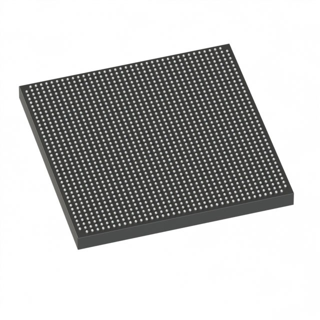
Stratix® V GS Field Programmable Gate Array (FPGA) IC 696 51200000 695000 1517-BBGA, FCBGA |
|---|---|
| Quantity | 106 Available (as of June 12, 2026) |

| Product Category | Field Programmable Gate Array (FPGA) |
|---|---|
| Manufacturer | Intel |
| Manufacturing Status | Obsolete |
| Manufacturer Standard Lead Time | Contact Us |
| Datasheet |
Specifications & Environmental
| Device Package | 1517-FBGA (40x40) | Grade | Commercial | Operating Temperature | 0°C – 85°C | ||
|---|---|---|---|---|---|---|---|
| Package / Case | 1517-BBGA, FCBGA | Number of I/O | 696 | Voltage | 870 mV - 930 mV | ||
| Mounting Method | Surface Mount | RoHS Compliance | RoHS Compliant | REACH Compliance | REACH Unknown | ||
| Moisture Sensitivity Level | 3 (168 Hours) | Number of LABs/CLBs | 262400 | Number of Logic Elements/Cells | 695000 | ||
| Number of Gates | N/A | ECCN | 3A001A2C | HTS Code | 8542.39.0001 | ||
| Qualification | N/A | Total RAM Bits | 51200000 |
Overview of 5SGSED8K1F40C2N – Stratix® V GS Field Programmable Gate Array (FPGA) IC, 695,000 logic elements
The 5SGSED8K1F40C2N is a Stratix V GS field programmable gate array (FPGA) optimized for transceiver-based, DSP-centric designs. Built on a 28‑nm architecture with an enhanced core and integrated hard IP, this device targets bandwidth- and compute-intensive applications that need high logic density and abundant on-chip memory.
Key platform attributes include approximately 695,000 logic elements, roughly 51.2 Mbits of embedded memory, and extensive I/O connectivity (696 pins). The GS variant is designed for high-precision DSP and transceiver applications where integrated multipliers and high-speed serial interfaces are required.
Key Features
- Core Architecture 28‑nm Stratix V architecture with an enhanced adaptive logic module (ALM) and comprehensive fabric clocking for high-performance logic implementation.
- Logic Capacity Approximately 695,000 logic elements to implement large, complex digital designs.
- Embedded Memory Approximately 51.2 Mbits of on-chip RAM (Total RAM Bits: 51,200,000) using M20K block architecture for buffer and storage needs.
- DSP Resources GS family devices include variable‑precision DSP blocks (series-level capability) for high‑throughput multiply/accumulate operations suited to signal processing workloads.
- Transceiver Capability (Series-Level) Stratix V GS devices offer integrated transceivers with multi‑gigabit data-rate capability suitable for backplane and optical interfaces (series-level specification).
- I/O and Package 696 user I/O pins in a 1517‑BBGA FCBGA package (supplier package: 1517‑FBGA, 40×40 mm) with surface-mount mounting for compact board-level integration.
- Power Core supply voltage range: 870 mV to 930 mV, enabling compatibility with defined power rail designs.
- Operating Temperature & Grade Commercial grade device rated for 0 °C to 85 °C operating temperature.
- Standards & Compliance RoHS compliant.
Typical Applications
- High‑performance DSP systems: Implementation of signal processing pipelines using the device's variable-precision DSP blocks and large logic capacity.
- Optical and backplane communications: Transceiver support at multi‑gigabit rates makes the device suitable for 40G/100G class transport and related interface modules.
- Network and packet processing: Large on-chip memory and abundant logic elements allow complex packet parsing, buffering, and traffic management functions.
- Broadcast and high‑performance computing: Compute‑intensive algorithms and dataflow architectures benefit from the device's DSP and embedded memory resources.
Unique Advantages
- High logic density: Approximately 695,000 logic elements let you consolidate large function blocks into a single FPGA, reducing system complexity.
- Substantial on‑chip memory: Around 51.2 Mbits of embedded RAM supports deep buffers and large working datasets without relying solely on external memory.
- DSP-optimized GS variant: Variable‑precision DSP blocks at the series level enable efficient implementation of high‑throughput multiply/accumulate and filtering functions.
- Broad I/O count and package: 696 I/O pins in a 1517‑BBGA FCBGA package provide extensive connectivity for multi-channel systems while maintaining a compact board footprint.
- Defined power envelope: Core voltage range of 870–930 mV allows predictable power-supply design and integration into existing power architectures.
- Commercial temperature rating: Rated for 0 °C to 85 °C operation for standard commercial deployments.
Why Choose 5SGSED8K1F40C2N?
The 5SGSED8K1F40C2N provides a balance of high logic capacity, significant on-chip memory, and DSP-focused resources in the Stratix V GS family—making it suitable for transceiver‑centric and compute‑heavy designs. Its package and I/O density support complex, multi‑channel systems while the defined core voltage and commercial temperature rating simplify platform engineering.
As a member of the Stratix V family, this device aligns with a scalable FPGA platform that includes hard IP and series‑level features aimed at bandwidth‑ and DSP‑oriented markets, supporting a streamlined path from prototyping to higher‑volume production options available for the family.
Request a quote or submit an inquiry for part number 5SGSED8K1F40C2N to discuss pricing, availability, and integration details for your design.


Date Founded: 1968
Headquarters: Santa Clara, California, USA
Employees: 130,000+
Revenue: $54.23 Billion
Certifications and Memberships: ISO9001:2015, ISO14001:2015, ISO17025:2017, ISO27001:2022, ISO45001:2018, ISO50001:2018


