
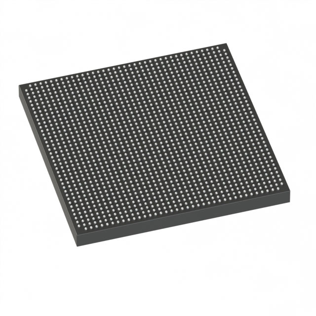
5SGSMD4K2F40I2LN
| Part Description |
Stratix® V GS Field Programmable Gate Array (FPGA) IC 696 19456000 360000 1517-BBGA, FCBGA |
|---|---|
| Quantity | 1,329 Available (as of October 8, 2026) |
| Product Category | Field Programmable Gate Array (FPGA) |
|---|---|
| Manufacturer | Intel |
| Manufacturing Status | Obsolete |
| Manufacturer Standard Lead Time | Contact Us |
| Datasheet |
Specifications & Environmental
| Device Package | 1517-FBGA (40x40) | Grade | Industrial | Operating Temperature | -40°C – 100°C | ||
|---|---|---|---|---|---|---|---|
| Package / Case | 1517-BBGA, FCBGA | Number of I/O | 696 | Voltage | 820 mV - 880 mV | ||
| Mounting Method | Surface Mount | RoHS Compliance | RoHS Compliant | REACH Compliance | REACH Unknown | ||
| Moisture Sensitivity Level | 3 (168 Hours) | Number of LABs/CLBs | 135840 | Number of Logic Elements/Cells | 360000 | ||
| Number of Gates | N/A | ECCN | 3A001A2C | HTS Code | 8542.39.0001 | ||
| Qualification | N/A | Total RAM Bits | 19456000 |
Overview of 5SGSMD4K2F40I2LN – Stratix V GS Field Programmable Gate Array (1517-BBGA, FCBGA)
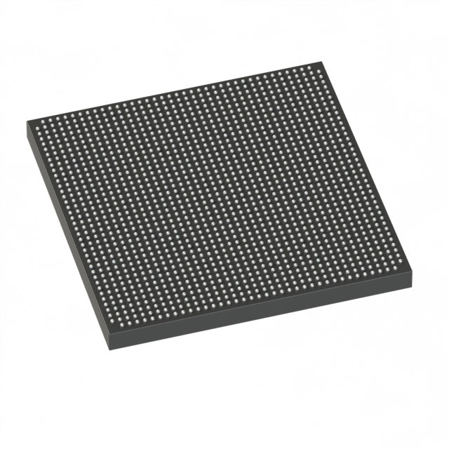
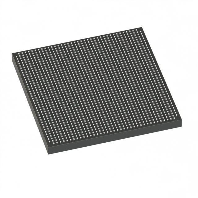
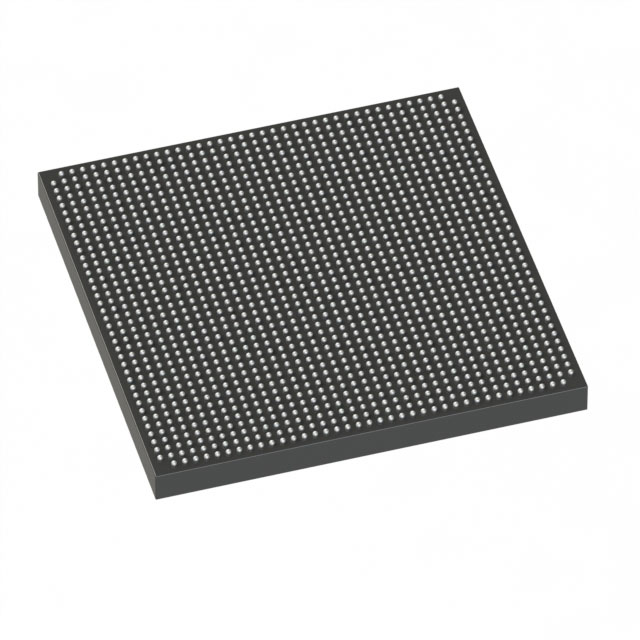
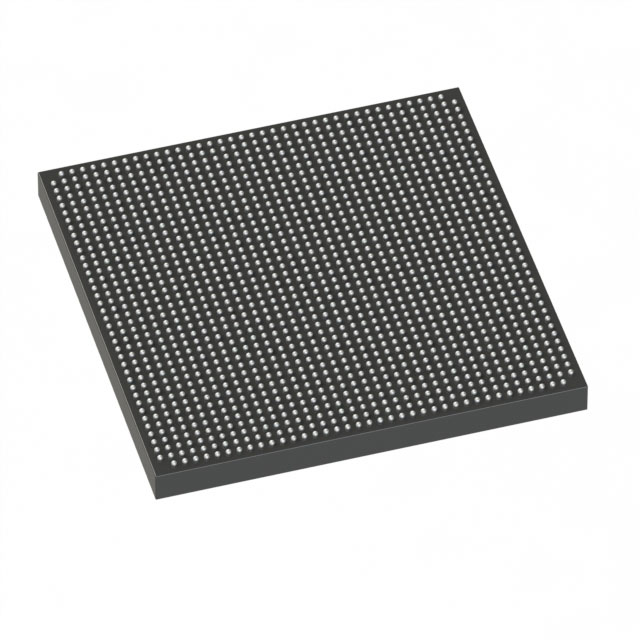
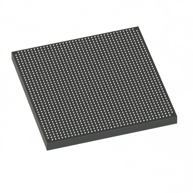
The 5SGSMD4K2F40I2LN is an Intel Stratix V GS field-programmable gate array (FPGA) in a 1517-BBGA FCBGA package. Built on a 28‑nm TSMC process, this GS‑variant device targets transceiver‑based, DSP‑centric designs and applications that require large logic capacity and significant embedded memory.
Its architecture combines a high logic element count, abundant variable‑precision DSP resources, and integrated high‑speed transceivers, making it suited for wireline, military, broadcast, and high‑performance computing applications where bandwidth and DSP throughput matter.
Key Features
- Logic Capacity Approximately 360,000 logic elements to implement complex digital designs and large FPGA fabrics.
- Embedded Memory Approximately 19.456 Mbits of on‑chip RAM backed by 20 Kbit (M20K) embedded memory blocks for buffering, lookup tables, and data staging.
- DSP Resources Stratix V GS devices include variable precision DSP blocks; the family supports up to 3,926 18×18 or 1,963 27×27 multipliers for high‑throughput signal processing workloads.
- Transceivers GS devices offer integrated transceivers with 14.1 Gbps data‑rate capability for high‑bandwidth serial interfaces and backplane/optical links.
- I/O and Packaging 696 general‑purpose I/O pins in a 1517‑BBGA (FCBGA) package; supplier package listed as 1517‑FBGA (40×40).
- Process and Hard IP 28‑nm process technology with an Embedded HardCopy Block for hardening IP such as PCIe Gen3/Gen2/Gen1 instantiations.
- Power Core supply voltage range: 820 mV to 880 mV, enabling integration with low‑voltage power domains.
- Industrial Temperature Range Operating temperature from −40 °C to 100 °C, suitable for industrial environments.
- Compliance RoHS‑compliant manufacturing.
Typical Applications
- High‑Performance Computing Accelerators and data‑plane processing where large logic and DSP resources deliver parallel computation and low‑latency processing.
- Wireline and Optical Transport Backplane and optical interface systems using high‑speed transceivers for 40G/100G class applications.
- Broadcast and Signal Processing Real‑time video/audio processing and modulation tasks leveraging variable‑precision DSP multipliers and abundant embedded memory.
- Military and Communications Systems DSP‑centric communications equipment that requires robust I/O count and operation across industrial temperature ranges.
Unique Advantages
- High Logic Density: Delivers approximately 360,000 logic elements to realize large, complex designs without partitioning across multiple devices.
- Substantial On‑Chip Memory: Approximately 19.456 Mbits of embedded RAM and M20K blocks reduce external memory dependencies and improve data locality.
- Dedicated DSP Fabric: Variable‑precision DSP blocks and family support for thousands of multipliers accelerate compute‑intensive signal processing tasks.
- Integrated High‑Speed I/O: GS‑class transceivers support 14.1 Gbps links for high‑bandwidth serial interfaces and system interconnects.
- Industrial‑Grade Thermal Range: −40 °C to 100 °C operation fits demanding environmental requirements for rugged equipment.
- IP Hardening Path: Embedded HardCopy Block capability provides a route to harden commonly used IP (for example PCIe) when migrating designs to ASICs.
Why Choose 5SGSMD4K2F40I2LN?
The 5SGSMD4K2F40I2LN balances large logic capacity, significant embedded memory, extensive DSP resources, and integrated transceiver capability within a single Stratix V GS device. It is positioned for engineers designing bandwidth‑ and DSP‑intensive systems that require a robust, industrial‑rated FPGA with a clear path to hardened IP and higher volume production strategies.
This device is well suited for teams building high‑performance compute, networking, broadcast, and communications systems that need dense logic, high I/O count, and reliable operation across a wide temperature range.
Request a quote or submit a purchase inquiry to receive pricing, availability, and lead‑time information for the 5SGSMD4K2F40I2LN. Our team can provide part availability and support for procurement and deployment planning.





















Date Founded: 1968
Headquarters: Santa Clara, California, USA
Employees: 130,000+
Revenue: $54.23 Billion
Certifications and Memberships: ISO9001:2015, ISO14001:2015, ISO17025:2017, ISO27001:2022, ISO45001:2018, ISO50001:2018


