
A3PN125-Z1VQG100I
| Part Description |
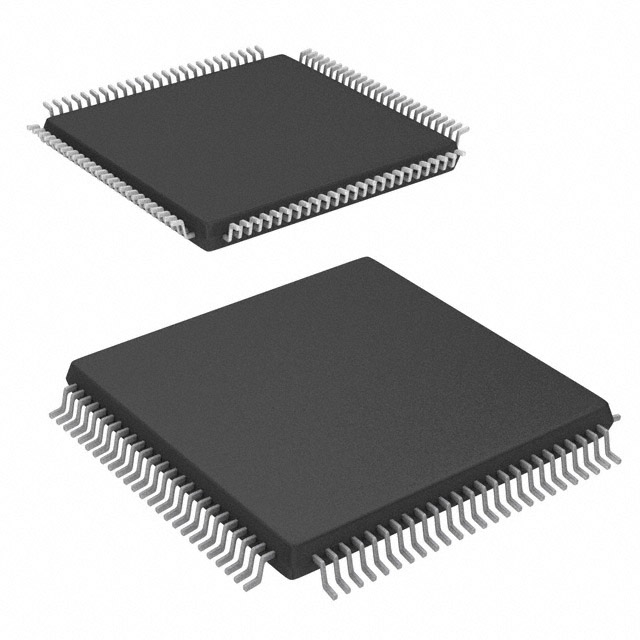
ProASIC3 nano Field Programmable Gate Array (FPGA) IC 71 36864 100-TQFP |
|---|---|
| Quantity | 275 Available (as of June 15, 2026) |

| Product Category | Field Programmable Gate Array (FPGA) |
|---|---|
| Manufacturer | Microchip Technology |
| Manufacturing Status | Obsolete |
| Manufacturer Standard Lead Time | Contact Us |
| Datasheet |
Specifications & Environmental
| Device Package | 100-VQFP (14x14) | Grade | Industrial | Operating Temperature | -40°C – 100°C | ||
|---|---|---|---|---|---|---|---|
| Package / Case | 100-TQFP | Number of I/O | 71 | Voltage | 1.425 V - 1.575 V | ||
| Mounting Method | Surface Mount | RoHS Compliance | Unknown | REACH Compliance | REACH Unaffected | ||
| Moisture Sensitivity Level | 3 (168 Hours) | Number of LABs/CLBs | 3072 | Number of Logic Elements/Cells | 3072 | ||
| Number of Gates | 125000 | ECCN | 3A991D | HTS Code | 8542.39.0001 | ||
| Qualification | N/A | Total RAM Bits | 36864 |
Overview of A3PN125-Z1VQG100I – ProASIC3 nano Field Programmable Gate Array (FPGA) IC 71 36864 100-TQFP
The A3PN125-Z1VQG100I is a ProASIC3 nano FPGA from Microchip Technology, offering a compact, mid-density programmable logic solution. It integrates approximately 3,072 logic elements (3072 logic elements), roughly 125,000 gates of combinational logic capacity, and on-chip memory to support embedded logic and buffering.
Designed with industrial-grade robustness, the device provides 71 user I/Os, a narrow core supply range of 1.425 V to 1.575 V, and an operating temperature span of -40°C to 100°C. The ProASIC3 nano family documentation highlights low-power modes and global resource features such as VersaNet global network distribution and spine architecture, enabling efficient system-level clocking and resource sharing.
Key Features
- Core Logic — Approximately 3,072 logic elements and 125,000 gates to implement combinational and sequential logic functions.
- Embedded Memory — Approximately 36,864 bits of on-chip RAM for small buffers, state storage, and local data paths.
- I/O — 71 programmable I/Os for interfacing with peripherals, sensors, and other digital subsystems.
- Power and Voltage — Core supply range of 1.425 V to 1.575 V; device documentation includes coverage of low-power modes to help manage static and dynamic power.
- Architecture & Global Resources — Device family documentation addresses global resource support, including VersaNet global network distribution, spine architecture, and clock aggregation for system-level integration.
- Package & Mounting — Supplied in a 100-pin TQFP package (supplier device package listed as 100-VQFP, 14 × 14 mm); surface-mount mounting for PCB assembly.
- Industrial Grade and Temperature Range — Rated as Industrial with an operating temperature range of -40°C to 100°C for demanding environments.
- Compliance — RoHS compliant for lead-free manufacturing processes.
Typical Applications
- Industrial Control — Implement control logic, finite-state machines, and I/O aggregation in systems that require industrial temperature operation and reliable on-board logic capacity.
- Embedded Interface & Glue Logic — Bridge peripherals and consolidate interface logic using the device’s 71 I/Os and integrated logic elements.
- Low-Power Embedded Systems — Use documented low-power modes and the device’s narrow supply range to optimize power consumption in energy-conscious designs.
- OEM Logic Integration — Integrate custom algorithmic or timing-critical functions on-chip to reduce component count and simplify PCB routing.
Unique Advantages
- Right-sized logic capacity: Approximately 3,072 logic elements and 125,000 gates provide a clear balance between integration and cost for mid-density designs.
- On-chip memory for local buffering: About 36,864 bits of embedded RAM reduce dependence on external memory for small data-storage needs.
- Deterministic I/O resources: 71 user I/Os enable predictable interfacing and simplify peripheral connectivity planning.
- Industrial-ready operation: Rated for -40°C to 100°C, supporting deployments in temperature-extreme environments.
- Power and system-level resource support: Narrow core voltage range and documented low-power modes help designers manage power budgets; architecture topics such as global resource distribution and clock aggregation aid system integration.
- Manufacturability and compliance: Surface-mount 100-pin TQFP package and RoHS compliance support standard assembly flows and regulatory requirements.
Why Choose A3PN125-Z1VQG100I?
The A3PN125-Z1VQG100I positions itself as a practical, industrial-grade ProASIC3 nano FPGA option for engineers seeking a compact programmable logic device with a clear balance of logic resources, on-chip memory, and I/O count. Its documented architecture and global resource topics—combined with low-power mode support—make it suitable for embedded control, interface consolidation, and OEM logic integration where predictable thermal and power behavior matter.
Backed by Microchip Technology’s ProASIC3 nano documentation and a RoHS-compliant manufacturing profile, this device is targeted at teams that need reliable, mid-density FPGA capability in a surface-mount 100-TQFP footprint with industrial temperature support.
Request a quote or submit a procurement inquiry to receive pricing, availability, and technical documentation for the A3PN125-Z1VQG100I.


Date Founded: 1989
Headquarters: Chandler, Arizona, USA
Employees: 22,000+
Revenue: $8.349 Billion
Certifications and Memberships: ISO9001:2015, IATF16949:2016, AS 9100D


