
A3PN125-Z2VQ100
| Part Description |
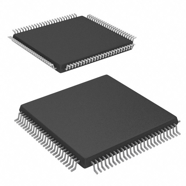
ProASIC3 nano Field Programmable Gate Array (FPGA) IC 71 36864 100-TQFP |
|---|---|
| Quantity | 714 Available (as of June 15, 2026) |
| Product Category | Field Programmable Gate Array (FPGA) |
|---|---|
| Manufacturer | Microchip Technology |
| Manufacturing Status | Obsolete |
| Manufacturer Standard Lead Time | Contact Us |
| Datasheet |
Specifications & Environmental
| Device Package | 100-VQFP (14x14) | Grade | Commercial | Operating Temperature | -20°C – 85°C | ||
|---|---|---|---|---|---|---|---|
| Package / Case | 100-TQFP | Number of I/O | 71 | Voltage | 1.425 V - 1.575 V | ||
| Mounting Method | Surface Mount | RoHS Compliance | RoHS non-compliant | REACH Compliance | REACH Unaffected | ||
| Moisture Sensitivity Level | 3 (168 Hours) | Number of LABs/CLBs | 3072 | Number of Logic Elements/Cells | 3072 | ||
| Number of Gates | 125000 | ECCN | 3A991D | HTS Code | 8542.39.0001 | ||
| Qualification | N/A | Total RAM Bits | 36864 |
Overview of A3PN125-Z2VQ100 – ProASIC3 nano FPGA, 71 I/Os, 36.9 kbit RAM, 100‑TQFP
The A3PN125-Z2VQ100 is a ProASIC3 nano Field Programmable Gate Array (FPGA) from Microchip Technology. It provides a flash-based FPGA fabric with 3,072 logic elements and 71 user I/Os in a compact 100‑TQFP (14×14) surface-mount package.
Designed for applications that require moderate logic density, on-chip embedded memory, and low-voltage operation, this commercial-grade device combines programmable logic capacity with a range of low-power features described in the ProASIC3 nano FPGA user documentation.
Key Features
- Logic Capacity Approximately 3,072 logic elements (cells) and 125,000 equivalent gates provide a programmable fabric for implementing custom control, glue logic, and finite-state machines.
- Embedded Memory Total on-chip RAM of 36,864 bits (approximately 36.9 kbits) for small buffers, FIFOs, and state storage.
- I/O 71 user I/O pins to support diverse peripheral interfacing and board-level signal routing requirements.
- Power and Voltage Specified core supply range from 1.425 V to 1.575 V to match low-voltage system rails.
- Low-Power Architecture ProASIC3 nano FPGA fabric documentation includes static, sleep and shutdown modes for reducing power in idle or low-activity conditions.
- Package and Mounting Available in a 100‑lead TQFP (14×14) surface-mount package (supplier device package shown as 100‑VQFP 14×14), enabling compact board integration.
- Operating Range and Grade Commercial grade device with an operating temperature range of −20 °C to 85 °C.
- Compliance RoHS‑compliant construction for regulatory and manufacturing consistency.
Typical Applications
- Embedded control and glue logic Implement custom control functions and board-level glue logic using the device’s ~3,072 logic elements and 71 I/Os.
- I/O expansion and protocol bridging Use the available I/O resources to bridge interfaces or expand peripheral connectivity on space-constrained PCBs.
- Low-power system functions Take advantage of documented low-power modes in the ProASIC3 nano fabric for designs that need reduced idle and sleep power.
- Compact FPGA integration 100‑TQFP surface-mount package fits compact designs where board area and standard SMT assembly are required.
Unique Advantages
- Right-sized logic capacity: Provides ~3,072 logic elements and 125,000 gates, delivering programmable resources suited to mid-range control and interface tasks without excessive overcapacity.
- On-chip embedded memory: Approximately 36.9 kbits of RAM enables local buffering and state retention without external memory, simplifying BOM and layout.
- Flexible I/O count: 71 user I/Os offer ample connectivity for sensors, peripherals, and custom interfaces while preserving pin-efficiency in a compact package.
- Low-voltage core operation: Narrow core supply window (1.425 V to 1.575 V) aligns with low-voltage system designs for consistent power planning.
- Compact package for SMT assembly: 100‑lead TQFP (14×14) surface-mount form factor eases placement on small PCBs and standard assembly lines.
- Regulatory readiness: RoHS compliance supports environmentally conscious manufacturing and supply-chain requirements.
Why Choose A3PN125-Z2VQ100?
The A3PN125-Z2VQ100 positions itself as a practical, flash-based programmable fabric for designers needing moderate logic density, embedded RAM, and a flexible I/O set in a compact surface-mount package. Its ProASIC3 nano FPGA architecture and documented low-power modes make it suitable for designs where power management and reliable programmable logic are required within commercial temperature ranges.
This device is well suited to engineering teams developing control logic, interface bridges, and board-level programmable functions that benefit from on-chip memory and a standard 100‑lead TQFP package. Its combination of logic resources, I/O count, and vendor-supported FPGA fabric documentation delivers a straightforward, scalable solution for mid-range embedded designs.
Request a quote or submit a procurement inquiry to evaluate A3PN125-Z2VQ100 for your next design.


Date Founded: 1989
Headquarters: Chandler, Arizona, USA
Employees: 22,000+
Revenue: $8.349 Billion
Certifications and Memberships: ISO9001:2015, IATF16949:2016, AS 9100D


