
A3PN250-Z1VQ100
| Part Description |
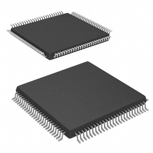
ProASIC3 nano Field Programmable Gate Array (FPGA) IC 68 36864 100-TQFP |
|---|---|
| Quantity | 1,074 Available (as of June 18, 2026) |

| Product Category | Field Programmable Gate Array (FPGA) |
|---|---|
| Manufacturer | Microchip Technology |
| Manufacturing Status | Obsolete |
| Manufacturer Standard Lead Time | Contact Us |
| Datasheet |
Specifications & Environmental
| Device Package | 100-VQFP (14x14) | Grade | Commercial | Operating Temperature | -20°C – 85°C | ||
|---|---|---|---|---|---|---|---|
| Package / Case | 100-TQFP | Number of I/O | 68 | Voltage | 1.425 V - 1.575 V | ||
| Mounting Method | Surface Mount | RoHS Compliance | RoHS non-compliant | REACH Compliance | REACH Unaffected | ||
| Moisture Sensitivity Level | 3 (168 Hours) | Number of LABs/CLBs | 6144 | Number of Logic Elements/Cells | 6144 | ||
| Number of Gates | 250000 | ECCN | 3A991D | HTS Code | 8542.39.0001 | ||
| Qualification | N/A | Total RAM Bits | 36864 |
Overview of A3PN250-Z1VQ100 – ProASIC3 nano Field Programmable Gate Array (FPGA) IC 68 I/O, 36,864‑bit RAM, 100‑TQFP
The A3PN250-Z1VQ100 is a ProASIC3 nano flash-based FPGA from Microchip Technology, offering a low-power programmable fabric tailored for commercial embedded designs. It combines a moderate logic capacity with on-chip RAM and 68 general-purpose I/Os in a 100‑pin TQFP surface-mount package.
Designed for applications that require configurable logic, flexible I/O and nonvolatile flash architecture, this device addresses use cases where compact footprint, low-voltage operation and commercial-grade temperature range are priorities.
Key Features
- Logic Capacity — 6,144 logic elements (cells) delivering up to 250,000 equivalent gates for implementing custom digital functions and control logic.
- Embedded Memory — 36,864 bits of on-chip RAM (approximately 36.9 kbits) for FIFOs, small buffers and state storage without external memory.
- I/O Count — 68 user I/Os to support a broad mix of external interfaces and peripheral connections.
- Flash-Based FPGA Fabric — ProASIC3 nano flash architecture and device documentation focused on low-power modes and flash-based global resources.
- Power — Single-core supply range of 1.425 V to 1.575 V for the programmable fabric.
- Package & Mounting — 100‑TQFP surface-mount package; supplier device package listed as 100‑VQFP (14×14 mm) for physical footprint reference.
- Environmental & Grade — Commercial grade device with RoHS compliance and an operating temperature range of −20 °C to 85 °C.
Typical Applications
- Embedded Control — Implement custom control logic and state machines using the device’s 6,144 logic elements and on-chip RAM to minimize external components.
- Sensor and Peripheral Interfaces — Use the 68 I/Os to aggregate sensors, actuators or peripherals in compact, low-voltage systems.
- Prototyping and Custom Logic — Rapidly iterate and validate custom digital functions with the reprogrammable flash fabric and surface-mount 100‑TQFP package for board-level evaluation.
Unique Advantages
- Moderate Logic Density in a Compact Package: 6,144 logic elements and 250,000 equivalent gates provide substantial programmable resources while fitting a 100‑pin TQFP footprint.
- On-Chip Memory Reduces BOM: 36,864 bits of embedded RAM allow local buffering and state retention, reducing the need for small external memories.
- Low-Voltage, Flash-Based Fabric: Flash architecture combined with a 1.425 V–1.575 V supply supports low-power modes described in the ProASIC3 nano documentation, helping manage system power budgets.
- Flexible I/O Count: Sixty-eight I/Os enable diverse peripheral and interface options without expanding package pin count.
- Commercial-Grade Thermal Range: Rated for −20 °C to 85 °C, matching many consumer and commercial embedded environments.
- RoHS Compliant: Meets RoHS requirements for lead-free assembly and regulatory considerations.
Why Choose A3PN250-Z1VQ100?
The A3PN250-Z1VQ100 positions itself as a practical, flash-based FPGA choice for commercial embedded designs that need moderate logic capacity, on-chip memory and a generous I/O set in a compact surface-mount package. Its ProASIC3 nano fabric and documented low-power modes make it suited for systems where power management and nonvolatile configuration matter.
Backed by Microchip Technology’s ProASIC3 nano documentation and a clear set of electrical and thermal specifications, this device is appropriate for engineers and procurement teams building commercial products that require configurable logic, a small BOM and predictable supply and temperature requirements.
Request a quote or submit a purchase inquiry for the A3PN250-Z1VQ100 to evaluate it for your next commercial embedded design.


Date Founded: 1989
Headquarters: Chandler, Arizona, USA
Employees: 22,000+
Revenue: $8.349 Billion
Certifications and Memberships: ISO9001:2015, IATF16949:2016, AS 9100D


