
A3PN250-VQG100
| Part Description |
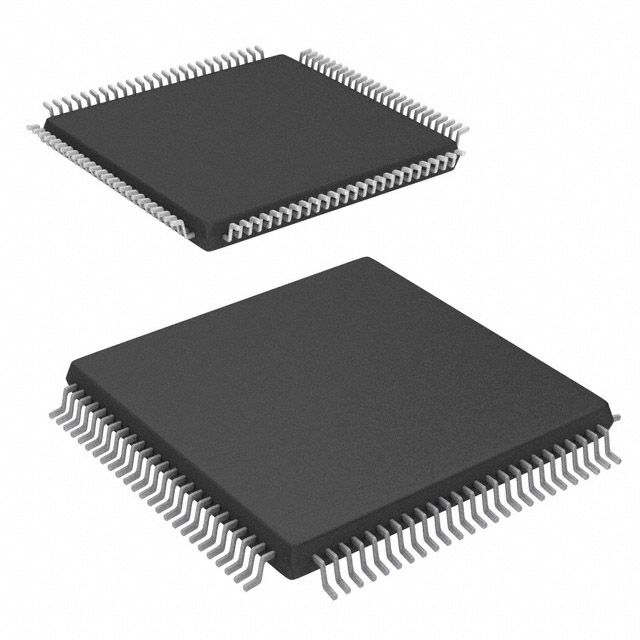
ProASIC3 nano Field Programmable Gate Array (FPGA) IC 68 36864 100-TQFP |
|---|---|
| Quantity | 1,588 Available (as of June 15, 2026) |

| Product Category | Field Programmable Gate Array (FPGA) |
|---|---|
| Manufacturer | Microchip Technology |
| Manufacturing Status | Active |
| Manufacturer Standard Lead Time | 8 Weeks |
| Datasheet |
Specifications & Environmental
| Device Package | 100-VQFP (14x14) | Grade | Commercial | Operating Temperature | -20°C – 85°C | ||
|---|---|---|---|---|---|---|---|
| Package / Case | 100-TQFP | Number of I/O | 68 | Voltage | 1.425 V - 1.575 V | ||
| Mounting Method | Surface Mount | RoHS Compliance | ROHS3 Compliant | REACH Compliance | REACH Unaffected | ||
| Moisture Sensitivity Level | 3 (168 Hours) | Number of LABs/CLBs | 6144 | Number of Logic Elements/Cells | 6144 | ||
| Number of Gates | 250000 | ECCN | 3A991D | HTS Code | 8542.39.0001 | ||
| Qualification | N/A | Total RAM Bits | 36864 |
Overview of A3PN250-VQG100 – ProASIC3 nano FPGA IC, 68 I/O, 36,864-bit RAM, 100-TQFP
The A3PN250-VQG100 is a ProASIC3 nano field programmable gate array (FPGA) from Microchip Technology. It provides a mid-density programmable logic fabric with 6,144 logic elements and on-chip embedded RAM to support compact, configurable digital designs.
Designed for commercial-grade embedded and consumer applications, the device combines a 250,000-gate equivalent fabric, 68 general-purpose I/Os and a compact 100-pin TQFP package to balance integration and board-space efficiency.
Key Features
- Core Logic 6,144 logic elements (LEs) providing mid-range programmable logic capacity suitable for glue logic, protocol bridges and control functions.
- Embedded Memory 36,864 bits of on-chip RAM for buffering, small FIFOs and local data storage within the FPGA fabric.
- I/O Count 68 general-purpose I/O pins to interface with peripherals, sensors and external logic devices.
- Logic Density Equivalent to 250,000 gates for implementing a variety of combinational and sequential logic functions.
- Power Supply Operates from a core voltage supply range of 1.425 V to 1.575 V, enabling compatibility with targeted board power rails.
- Package & Mounting Available in a 100-pin TQFP package (supplier device package: 100-VQFP, 14×14) and designed for surface-mount assembly.
- Temperature & Grade Commercial grade device rated for an operating temperature range of −20 °C to 85 °C.
- Compliance RoHS-compliant manufacturing for lead-free assembly and regulatory alignment.
Typical Applications
- Consumer Electronics Implement control logic, user-interface handling or peripheral bridging in compact consumer devices using the 100-TQFP footprint.
- Embedded Systems Provide mid-range programmable logic and local RAM for embedded control, protocol adaptation and I/O consolidation.
- Communications & Networking Implement interface bridging, simple packet handling or timing logic leveraging 68 I/O pins and on-chip RAM.
- Prototyping and Low-Volume Production Suitable for rapid development and deployment where a commercial-grade, surface-mount FPGA is required in a small package.
Unique Advantages
- Balanced Logic Capacity: 6,144 logic elements provide sufficient resources for a wide range of mid-density designs without excessive complexity.
- On-Chip RAM: 36,864 bits of embedded memory enable local buffering and small data storage without external memory components.
- Compact Package: 100-pin TQFP (14×14) in a surface-mount form factor simplifies PCB layout for space-constrained applications.
- Generous I/O Count: 68 I/O pins allow flexible connectivity to peripherals, sensors and external logic devices.
- Commercial Temperature Range: Rated for −20 °C to 85 °C to meet typical commercial application environments.
- Regulatory Alignment: RoHS compliance supports lead-free manufacturing and environmental requirements.
Why Choose A3PN250-VQG100?
The A3PN250-VQG100 is positioned as a commercially graded, mid-density FPGA that delivers a practical mix of logic elements, embedded RAM and I/O in a compact 100-TQFP package. It is well suited to engineers seeking a programmable solution for embedded and consumer applications where board space, programmable flexibility and a defined operating voltage range are important.
Built by Microchip Technology and offering clear, verifiable specifications—6,144 logic elements, 36,864 bits of RAM, 68 I/Os, and a 1.425–1.575 V core supply—the device provides predictable capacity for designs that require on-chip memory, moderate gate counts and a surface-mount package.
Request a quote or submit an inquiry to our sales team to check availability, lead times and pricing for the A3PN250-VQG100.


Date Founded: 1989
Headquarters: Chandler, Arizona, USA
Employees: 22,000+
Revenue: $8.349 Billion
Certifications and Memberships: ISO9001:2015, IATF16949:2016, AS 9100D


