
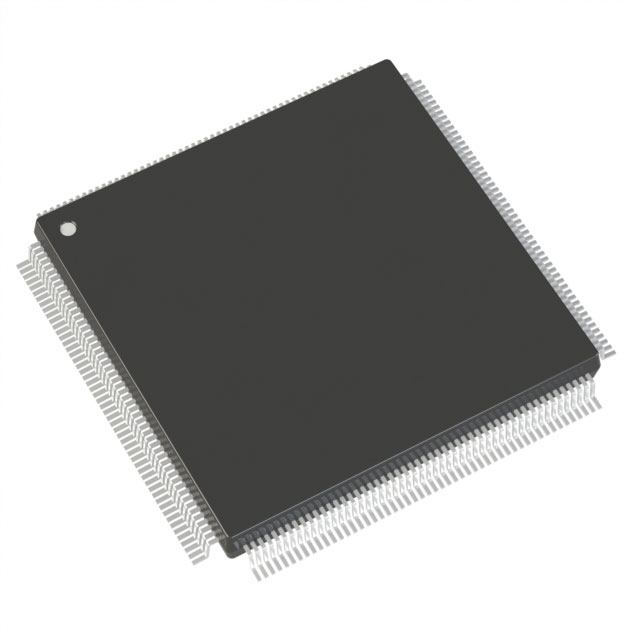
A54SX16A-1PQG208I
| Part Description |
SX-A Field Programmable Gate Array (FPGA) IC 175 208-BFQFP |
|---|---|
| Quantity | 1,370 Available (as of June 15, 2026) |
| Product Category | Field Programmable Gate Array (FPGA) |
|---|---|
| Manufacturer | Microchip Technology |
| Manufacturing Status | Active |
| Manufacturer Standard Lead Time | 14 Weeks |
| Datasheet |
Specifications & Environmental
| Device Package | 208-PQFP (28x28) | Grade | Industrial | Operating Temperature | -40°C – 85°C | ||
|---|---|---|---|---|---|---|---|
| Package / Case | 208-BFQFP | Number of I/O | 175 | Voltage | 2.25 V - 5.25 V | ||
| Mounting Method | Surface Mount | RoHS Compliance | ROHS3 Compliant | REACH Compliance | REACH Unaffected | ||
| Moisture Sensitivity Level | 3 (168 Hours) | Number of LABs/CLBs | 1452 | Number of Logic Elements/Cells | 1452 | ||
| Number of Gates | 24000 | ECCN | 3A991D | HTS Code | 8542.39.0001 | ||
| Qualification | N/A |
Overview of A54SX16A-1PQG208I – SX-A Field Programmable Gate Array (FPGA) IC 175 208-BFQFP
The A54SX16A-1PQG208I is a member of the SX-A family of nonvolatile, single‑chip FPGAs. It provides 24,000 system gates implemented as approximately 1,452 logic elements with up to 175 user‑programmable I/O pins in a 208‑pin quad flat package.
Designed for industrial environments, this device targets applications that require deterministic, reconfigurable logic with mixed‑voltage I/O capability and hot‑swap friendly interfaces. Core advantages include single‑chip nonvolatile configuration, configurable I/O voltages, and industry temperature grading for robust operation.
Key Features
- Logic Capacity — Approximately 1,452 logic elements corresponding to 24,000 system gates, enabling medium‑complexity programmable logic implementations.
- User I/O — Up to 175 user‑programmable I/Os, supporting flexible interfacing in dense I/O designs.
- Nonvolatile Single‑Chip Configuration — SX‑A family single‑chip, nonvolatile architecture for retained configuration without external memory.
- Configurable I/O and Mixed‑Voltage Support — Configurable I/O support described by the SX‑A family including 3.3 V / 5 V PCI, 5 V TTL, 3.3 V LVTTL, and 2.5 V LVCMOS2; device supply range 2.25 V to 5.25 V.
- Performance — Family performance characteristics include up to 250 MHz system performance and up to 350 MHz internal performance as documented for SX‑A devices.
- Package — 208‑pin BFQFP package (supplier device package listed as 208‑PQFP, 28×28), suitable for surface‑mount assembly.
- Industrial Temperature Grade — Rated for operation from −40 °C to +85 °C.
- Power and I/O Robustness — Hot‑swap compliant I/Os and power‑up/power‑down friendly operation (no sequencing required for supply voltages) as noted for the SX‑A family.
- No On‑Chip RAM — Total RAM bits: 0 (no embedded RAM reported for this device).
- Security and Testability — Family features include FuseLock secure programming technology and IEEE 1149.1 (JTAG) boundary‑scan testing capability.
- Standards and Tools — SX‑A family supports deterministic timing and in‑system diagnostics with Silicon Explorer II (as documented for the family).
- RoHS Compliant — Device is RoHS compliant.
Typical Applications
- Industrial Control — Use the industrial temperature rating and flexible I/O to implement control logic and interface conversions in factory and process automation equipment.
- Mixed‑Voltage Interface Bridging — Configurable I/O and 5 V input tolerance allow implementation of level‑translation and protocol bridging between legacy 5 V logic and modern lower‑voltage domains.
- PCI‑Related Logic — SX‑A family devices document 66 MHz PCI compliance and 3.3 V/5 V PCI I/O support, making the device suitable for PCI interface glue logic and protocol handling.
- Deterministic Timing Designs — Deterministic, user‑controllable timing features are suited for designs that require predictable timing behavior and in‑system verification.
Unique Advantages
- Nonvolatile, Single‑Chip Solution: Retains configuration without external configuration memory, simplifying board-level design and reducing BOM.
- Flexible I/O Voltage Support: Configurable I/O standards and a broad supply range (2.25 V to 5.25 V) enable direct interfacing to multiple logic families.
- Industrial Reliability: Specified operation from −40 °C to +85 °C for deployment in industrial temperature environments.
- Built‑In Security and Test: Family features such as FuseLock programming and JTAG boundary‑scan support protect IP and simplify manufacturing test.
- Hot‑Swap and Power‑Cycle Robustness: Hot‑swap compliant I/Os and no required supply sequencing reduce system complexity for hot‑plug or multi‑rail systems.
- Compact, High‑I/O Package: 208‑pin PQFP/BFQFP package provides up to 175 user I/Os in a surface‑mount form factor for space‑constrained boards.
Why Choose A54SX16A-1PQG208I?
The A54SX16A-1PQG208I combines the SX‑A family’s nonvolatile, single‑chip FPGA architecture with industrial temperature rating and flexible I/O options to address medium‑complexity programmable logic needs. With approximately 1,452 logic elements, up to 175 user I/Os, and robust I/O features, it is suited to designs requiring deterministic timing, mixed‑voltage interfacing, and secure configuration retention.
This device is appropriate for engineering teams and procurement seeking a compact FPGA solution that simplifies system design through integrated nonvolatile configuration, configurable I/O standards, and test/security features documented for the SX‑A family.
Request a quote or submit your procurement inquiry to receive pricing and availability for the A54SX16A-1PQG208I. Our team can provide lead‑time details and support for your design evaluation.


Date Founded: 1989
Headquarters: Chandler, Arizona, USA
Employees: 22,000+
Revenue: $8.349 Billion
Certifications and Memberships: ISO9001:2015, IATF16949:2016, AS 9100D


