
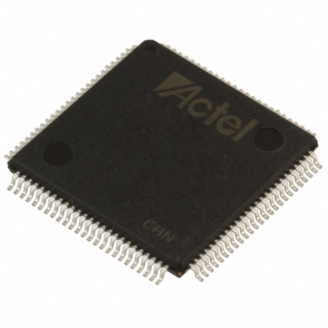
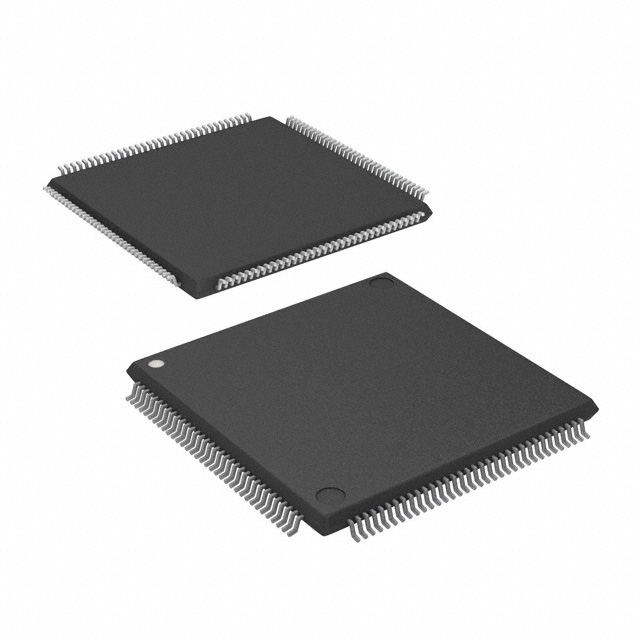
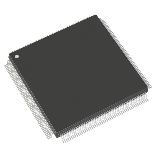
A54SX16A-1TQ100M
| Part Description |
SX-A Field Programmable Gate Array (FPGA) IC 81 100-LQFP |
|---|---|
| Quantity | 80 Available (as of June 15, 2026) |

| Product Category | Field Programmable Gate Array (FPGA) |
|---|---|
| Manufacturer | Microchip Technology |
| Manufacturing Status | Obsolete |
| Manufacturer Standard Lead Time | Contact Us |
| Datasheet |
Specifications & Environmental
| Device Package | 100-TQFP (14x14) | Grade | Military | Operating Temperature | -55°C – 125°C | ||
|---|---|---|---|---|---|---|---|
| Package / Case | 100-LQFP | Number of I/O | 81 | Voltage | 2.25 V - 5.25 V | ||
| Mounting Method | Surface Mount | RoHS Compliance | RoHS non-compliant | REACH Compliance | REACH Unaffected | ||
| Moisture Sensitivity Level | 3 (168 Hours) | Number of LABs/CLBs | 1452 | Number of Logic Elements/Cells | 1452 | ||
| Number of Gates | 24000 | ECCN | 3A001A2C | HTS Code | 8542.39.0001 | ||
| Qualification | N/A |
Overview of A54SX16A-1TQ100M – SX-A Field Programmable Gate Array (FPGA) IC 81 100-LQFP
The A54SX16A-1TQ100M is a member of the SX-A family of nonvolatile, single‑chip FPGAs from Microchip Technology. It provides 24,000 system gates across 1,452 logic elements with up to 81 user I/Os in a surface‑mount 100‑pin package, targeted at applications that require reprogrammable logic with integrated configuration and hardware security.
Designed for robust operation, this military‑grade device supports a wide supply range (2.25 V to 5.25 V) and an operating temperature range of −55 °C to 125 °C, making it suitable for designs that demand wide temperature tolerance and mixed‑voltage I/O flexibility.
Key Features
- Core Capacity — 24,000 system gates implemented across 1,452 logic elements, providing mid‑range programmable logic for glue‑logic, protocol handling, and control functions.
- I/O and Interface Flexibility — 81 user I/Os with configurable support for 3.3 V/5 V PCI, 5 V TTL, 3.3 V LVTTL and 2.5 V LVCMOS2; supports mixed‑voltage operation with 5 V input tolerance and 5 V drive strength.
- Performance — SX‑A family performance characteristics include up to 250 MHz system performance and up to 350 MHz internal performance (family specification).
- Configuration and Security — Nonvolatile, single‑chip configuration with Actel Secure Programming Technology (FuseLock™) to protect bitstreams and prevent reverse engineering (family feature).
- System and Testability — Boundary‑scan testing compliant with IEEE 1149.1 (JTAG) and in‑system diagnostic capability with Silicon Explorer II (family feature), enabling easier board‑level test and validation.
- Power and Reliability — Hot‑swap compliant I/Os and power‑up/power‑down friendly behavior (no sequencing required for supply voltages), simplifying system power sequencing.
- Package and Mounting — Surface‑mount 100‑LQFP package case; supplier device package listed as 100‑TQFP (14×14 mm).
- Environmental Compliance — RoHS compliant.
Typical Applications
- Mixed‑Voltage Interface Modules — Use the configurable I/Os and 5 V tolerance to bridge or adapt signals between 2.5 V, 3.3 V and 5 V domains.
- PCI‑Based Embedded Systems — Deploy where 66 MHz PCI compliance and programmable logic are required for interface logic, protocol adaptation, or peripheral glue logic.
- Military and Rugged Electronics — Leverage the military grade designation and −55 °C to 125 °C operating range for designs requiring wide temperature operation.
- Secure In‑System Programmable Designs — Apply the device where nonvolatile configuration and FuseLock™ security are needed to protect intellectual property and enable field updates.
Unique Advantages
- Integrated Nonvolatile Configuration: Single‑chip FPGA architecture removes the need for external configuration memory, simplifying board design and lowering component count.
- Flexible Mixed‑Voltage I/O: Configurable I/O support across common voltage standards and 5 V input tolerance make the device adaptable to diverse system interfaces.
- Robust Temperature Performance: Military grade and a −55 °C to 125 °C operating range support demanding environmental requirements and extended‑life deployments.
- Deterministic Timing and Resource Control: Family features include deterministic, user‑controllable timing and support for 100% resource utilization and pin locking, aiding predictable system behavior.
- Security and Testability: Built‑in secure programming (FuseLock™) and IEEE 1149.1 boundary‑scan support simplify IP protection and board‑level test flows.
- Broad Supply Range: Operates from 2.25 V to 5.25 V, allowing flexible power architectures and compatibility with a range of system rails.
Why Choose A54SX16A-1TQ100M?
The A54SX16A-1TQ100M positions itself as a mid‑capacity, nonvolatile FPGA option for systems that require secure, reprogrammable logic with robust environmental tolerance. Its combination of 24,000 system gates, 1,452 logic elements and flexible I/O makes it suitable for mixed‑voltage interfaces, PCI‑compatible subsystems, and military or rugged applications where temperature range and reliability are critical.
Backed by the SX‑A family feature set—nonvolatile single‑chip configuration, boundary‑scan testability, deterministic timing controls and secure programming—this device offers a compact, integration‑friendly solution that reduces external components while providing the configuration security and test support needed for long‑life designs.
Request a quote or contact sales to discuss pricing, availability, and how A54SX16A-1TQ100M can fit into your next design.


Date Founded: 1989
Headquarters: Chandler, Arizona, USA
Employees: 22,000+
Revenue: $8.349 Billion
Certifications and Memberships: ISO9001:2015, IATF16949:2016, AS 9100D


