
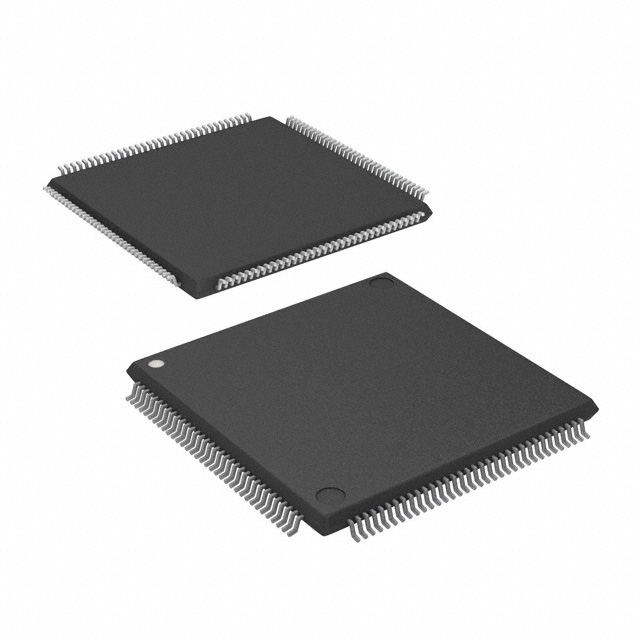
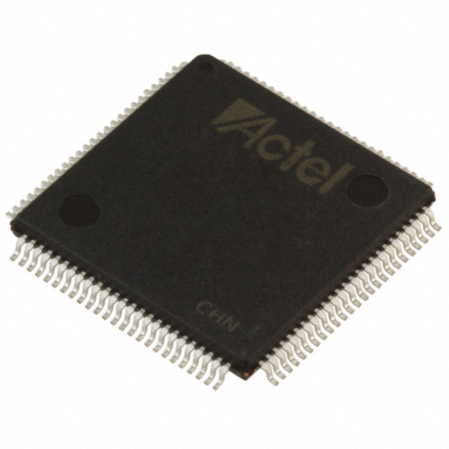
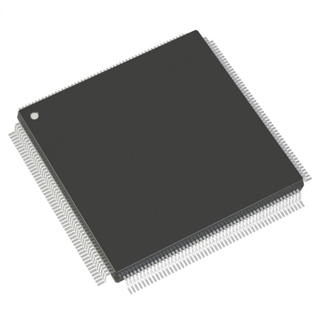
A54SX16A-1TQ144
| Part Description |
SX-A Field Programmable Gate Array (FPGA) IC 113 144-LQFP |
|---|---|
| Quantity | 932 Available (as of June 15, 2026) |
| Product Category | Field Programmable Gate Array (FPGA) |
|---|---|
| Manufacturer | Microchip Technology |
| Manufacturing Status | Obsolete |
| Manufacturer Standard Lead Time | Contact Us |
| Datasheet |
Specifications & Environmental
| Device Package | 144-TQFP (20x20) | Grade | Commercial | Operating Temperature | 0°C – 70°C | ||
|---|---|---|---|---|---|---|---|
| Package / Case | 144-LQFP | Number of I/O | 113 | Voltage | 2.25 V - 5.25 V | ||
| Mounting Method | Surface Mount | RoHS Compliance | RoHS non-compliant | REACH Compliance | REACH Unaffected | ||
| Moisture Sensitivity Level | 3 (168 Hours) | Number of LABs/CLBs | 1452 | Number of Logic Elements/Cells | 1452 | ||
| Number of Gates | 24000 | ECCN | 3A991D | HTS Code | 8542.39.0001 | ||
| Qualification | N/A |
Overview of A54SX16A-1TQ144 – SX-A Field Programmable Gate Array (FPGA) IC 113 144-LQFP
The A54SX16A-1TQ144 is a member of the SX-A family of nonvolatile single-chip FPGAs. This commercial-grade device provides 24,000 system gates implemented as 1,452 logic elements with 113 user I/Os in a 144-pin package.
Designed for mixed-voltage embedded and interface applications, the device offers configurable I/O support and family-level features such as hot-swap–capable I/Os, JTAG boundary-scan, and on-chip security options tailored for designs that require deterministic timing and persistent configuration.
Key Features
- Logic Capacity — 24,000 system gates realized as 1,452 logic elements for medium-complexity gate-array designs.
- User I/O — 113 user-programmable I/Os with configurable I/O support for mixed-voltage operation and 5 V input tolerance.
- Nonvolatile Single-Chip Configuration — Family-level single-chip nonvolatile architecture provides persistent configuration without external configuration memory.
- Performance — Family data cites up to 250 MHz system performance and up to 350 MHz internal performance for timing-sensitive logic.
- Voltage and Power — Wide supply range from 2.25 V to 5.25 V and power-up/power-down friendly behavior that requires no sequencing of supply voltages.
- Package and Mounting — 144-pin LQFP package (supplier device package: 144-TQFP, 20 × 20); surface-mount mounting type suitable for PCB assembly.
- Temperature and Grade — Commercial temperature grade, rated 0 °C to 70 °C.
- Security and Test — Family features include Actel Secure Programming technology with FuseLock™ for protection against reverse engineering and IEEE 1149.1 JTAG boundary-scan testing support.
- RoHS Compliance — Device is RoHS compliant.
- On-chip Memory — No embedded RAM (total on-chip RAM bits: 0), enabling predictable resource planning for designs that use external memory or register-based logic.
Typical Applications
- Mixed-Voltage Interface Bridging — Use the device’s configurable I/Os and 5 V tolerance to bridge between 5 V and lower-voltage logic domains for legacy interface support.
- PCI-Compatible System Logic — The family’s 66 MHz PCI compliance and configurable I/O make the device suitable for implementing PCI-compliant glue logic and interface control.
- Embedded Control and Glue Logic — 1,452 logic elements provide capacity for state machines, protocol handling, and peripheral control in embedded systems.
- Designs Requiring Persistent Configuration — Nonvolatile single-chip configuration is suited for applications that need immediate-on programmable logic without external configuration memory.
Unique Advantages
- Persistent, Single-Chip FPGA: Eliminates the need for external configuration memory, simplifying the bill of materials and board-level design.
- Mixed-Voltage Flexibility: Support for 2.5 V, 3.3 V and 5 V operation with 5 V input tolerance enables flexible interfacing to multiple voltage domains.
- Security Features: FuseLock™ secure programming reduces risk of reverse engineering and protects intellectual property in deployed systems.
- Testability and Diagnostics: IEEE 1149.1 JTAG boundary-scan and family in-system diagnostic/verification capabilities support production testing and field troubleshooting.
- Predictable Resource Model: Fixed logic element count and no embedded RAM simplify resource planning and deterministic timing analysis for control-dominated designs.
- RoHS Compliant: Supports regulatory requirements for lead-free assemblies.
Why Choose A54SX16A-1TQ144?
The A54SX16A-1TQ144 positions itself as a medium-capacity, commercial-temperature FPGA option within the SX-A family, offering 24,000 system gates and 1,452 logic elements in a compact 144-pin package. Its nonvolatile single-chip configuration, mixed-voltage I/O support, and on-chip security features make it a practical choice for embedded systems and interface logic where persistent configuration, I/O flexibility, and testability matter.
Design teams targeting predictable timing, simplified board-level BOM, and family scalability can leverage this device alongside other SX-A family members to match capacity and I/O needs across product variants while maintaining a consistent architecture and feature set.
If you would like pricing, availability, or to request a quote for the A54SX16A-1TQ144, submit a procurement inquiry and our team will respond with the next steps.


Date Founded: 1989
Headquarters: Chandler, Arizona, USA
Employees: 22,000+
Revenue: $8.349 Billion
Certifications and Memberships: ISO9001:2015, IATF16949:2016, AS 9100D


