
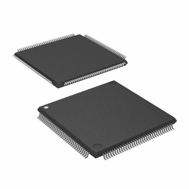
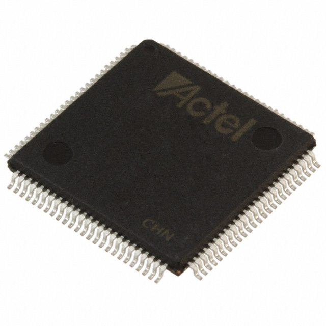
A54SX16A-1TQ144M
| Part Description |
SX-A Field Programmable Gate Array (FPGA) IC 113 144-LQFP |
|---|---|
| Quantity | 48 Available (as of June 10, 2026) |

| Product Category | Field Programmable Gate Array (FPGA) |
|---|---|
| Manufacturer | Microchip Technology |
| Manufacturing Status | Obsolete |
| Manufacturer Standard Lead Time | Contact Us |
| Datasheet |
Specifications & Environmental
| Device Package | 144-TQFP (20x20) | Grade | Military | Operating Temperature | -55°C – 125°C | ||
|---|---|---|---|---|---|---|---|
| Package / Case | 144-LQFP | Number of I/O | 113 | Voltage | 2.25 V - 5.25 V | ||
| Mounting Method | Surface Mount | RoHS Compliance | RoHS non-compliant | REACH Compliance | REACH Unaffected | ||
| Moisture Sensitivity Level | 3 (168 Hours) | Number of LABs/CLBs | 1452 | Number of Logic Elements/Cells | 1452 | ||
| Number of Gates | 24000 | ECCN | 3A001A2C | HTS Code | 8542.39.0001 | ||
| Qualification | N/A |
Overview of A54SX16A-1TQ144M – SX-A Field Programmable Gate Array (FPGA) IC 113 144-LQFP
The A54SX16A-1TQ144M is a military-grade SX-A family FPGA from Microchip Technology, provided in a 144-pin LQFP/TQFP package. It delivers a nonvolatile, single-chip programmable logic solution with approximately 1,452 logic elements and 24,000 system gates, designed for applications that require secure, deterministic logic in demanding temperature and power environments.
This device supports mixed-voltage operation across a wide supply range and a full military temperature grade, making it suitable for embedded systems that demand reliability, in-system programmability and on-board security features.
Key Features
- Logic Capacity — Approximately 1,452 logic elements and 24,000 system gates provide a compact programmable-logic resource for control, glue logic and custom state machines.
- I/O Count and Configurability — 113 user I/O pins with series-family configurable I/O options; supports multiple interface voltage standards across mixed-voltage designs.
- Nonvolatile Single-Chip Solution — SX-A family nonvolatile architecture removes the need for external configuration memory, simplifying board design and startup behavior.
- Security and Testability — Includes family-level secure programming (FuseLock™) to mitigate reverse engineering and supports IEEE 1149.1 boundary-scan (JTAG) for board-level test and diagnostics.
- Power and I/O Handling — Hot-swap compliant I/Os and power-up/power-down friendly operation that requires no special sequencing for supply voltages.
- Voltage Range — Operates from 2.25 V to 5.25 V, enabling flexible integration with a variety of system power rails.
- Package and Mounting — 144-LQFP package case (supplier device package listed as 144-TQFP 20×20) with surface-mount mounting for compact PCB designs.
- Temperature and Grade — Military grade with an operating temperature range of −55°C to 125°C for deployment in harsh environments.
- On-Chip Memory — No embedded RAM bits (Total RAM Bits: 0), which makes the device suitable for deterministic, register- and logic-centric designs.
- Standards and Family Performance — SX-A family capabilities include deterministic timing control, boundary-scan support and family performance characteristics documented in the SX-A datasheet.
- RoHS Compliant — Device is RoHS compliant for environmental regulatory considerations.
Typical Applications
- Military and Aerospace Systems — Military-grade temperature range and packaging suitability for embedded processing, protocol bridging and mission-critical control logic.
- Secure Embedded Controllers — Nonvolatile single-chip programming and FuseLock™ secure programming make the device appropriate for systems requiring on-board configuration security.
- Industrial Control and Automation — Deterministic timing and wide voltage tolerance support motor control, sensor interface and real-time I/O conditioning in harsh environments.
- Communications and Test Equipment — Boundary-scan support and configurable I/Os assist in board-level testability and protocol interface customization.
Unique Advantages
- Nonvolatile configuration — Eliminates external configuration memory and streamlines system boot and maintenance.
- Military-grade robustness — Rated for −55°C to 125°C and specified as a military-grade device for deployment in temperature-extreme applications.
- Flexible voltage operation — 2.25 V to 5.25 V supply range enables easy integration with diverse power domains and legacy interfaces.
- On-board security features — Family-level FuseLock™ secure programming helps protect intellectual property and mitigate reverse engineering risks.
- Testability and diagnostics — IEEE 1149.1 JTAG boundary-scan support improves manufacturing test coverage and in-system diagnostics.
- Compact surface-mount package — 144-pin LQFP/TQFP packaging provides a space-efficient footprint for constrained PCBs.
Why Choose A54SX16A-1TQ144M?
The A54SX16A-1TQ144M combines the SX-A family’s nonvolatile single-chip FPGA architecture with military-grade temperature and packaging to provide a reliable, secure programmable logic element for demanding embedded systems. Its mix of configurable I/O, deterministic timing characteristics and built-in security and test features make it well suited to applications where long-term robustness and on-board programmability are priorities.
This device is aimed at engineers and procurement teams designing compact, secure control and interface solutions that require a stable logic resource without external configuration components, and where board-level testability and environmental resilience are essential.
Request a quote or submit a product inquiry to receive pricing and availability information for the A54SX16A-1TQ144M.


Date Founded: 1989
Headquarters: Chandler, Arizona, USA
Employees: 22,000+
Revenue: $8.349 Billion
Certifications and Memberships: ISO9001:2015, IATF16949:2016, AS 9100D


