
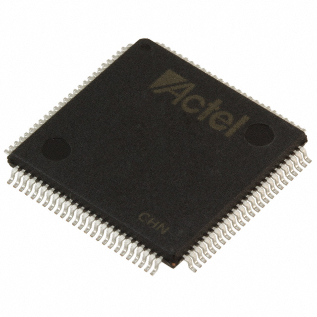
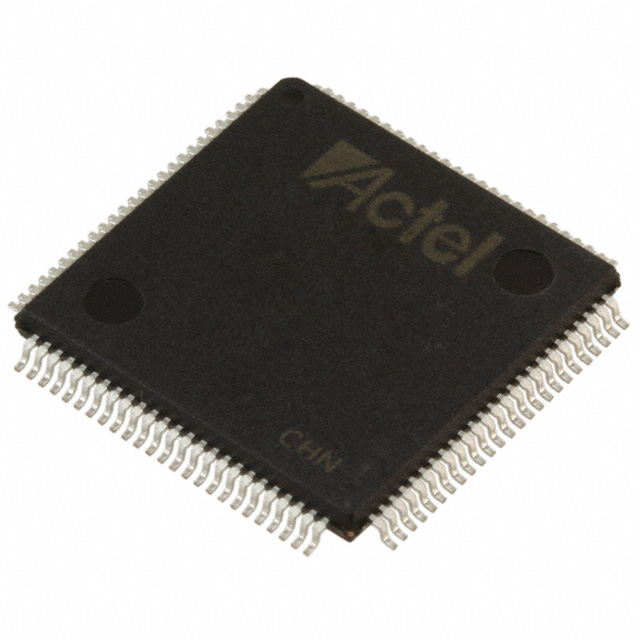
A54SX16A-1TQG100M
| Part Description |
SX-A Field Programmable Gate Array (FPGA) IC 81 100-LQFP |
|---|---|
| Quantity | 332 Available (as of October 8, 2026) |
| Product Category | Field Programmable Gate Array (FPGA) |
|---|---|
| Manufacturer | Microchip Technology |
| Manufacturing Status | Active |
| Manufacturer Standard Lead Time | 20 Weeks |
| Datasheet |
Specifications & Environmental
| Device Package | 100-TQFP (14x14) | Grade | Military | Operating Temperature | -55°C – 125°C | ||
|---|---|---|---|---|---|---|---|
| Package / Case | 100-LQFP | Number of I/O | 81 | Voltage | 2.25 V - 5.25 V | ||
| Mounting Method | Surface Mount | RoHS Compliance | ROHS3 Compliant | REACH Compliance | REACH Unaffected | ||
| Moisture Sensitivity Level | 3 (168 Hours) | Number of LABs/CLBs | 1452 | Number of Logic Elements/Cells | 1452 | ||
| Number of Gates | 24000 | ECCN | 3A001A2C | HTS Code | 8542.39.0001 | ||
| Qualification | N/A |
Overview of A54SX16A-1TQG100M – SX-A Field Programmable Gate Array (FPGA) IC 81 100-LQFP
The A54SX16A-1TQG100M is a military-grade SX-A family FPGA offering 24,000 system gates and 1,452 logic elements in a 100-pin LQFP package. It delivers a nonvolatile, single-chip FPGA architecture with configurable I/O and a broad supply range, designed for embedded systems requiring deterministic timing and rugged operating conditions.
Typical uses include embedded control and interface functions where secure in-system programmability, mixed-voltage I/O support, and extended temperature operation are required. The device combines mid-range logic capacity with series-level capabilities such as hot-swap compliant I/Os, JTAG boundary-scan, and secure programming features.
Key Features
- Logic Capacity — 24,000 system gates and 1,452 logic elements provide mid-range programmable logic resources for control, glue-logic and interface designs.
- I/O Density & Flexibility — 81 user I/Os with configurable I/O supporting 3.3 V/5 V PCI, 5 V TTL, 3.3 V LVTTL and 2.5 V LVCMOS2 signaling and individual output slew-rate control.
- Performance — Series-level performance indicators list up to 250 MHz system performance and up to 350 MHz internal performance for timing-critical functions.
- Power & Supply — Wide supply tolerance from 2.25 V to 5.25 V and power-up/down friendly behavior that does not require sequencing of supply rails.
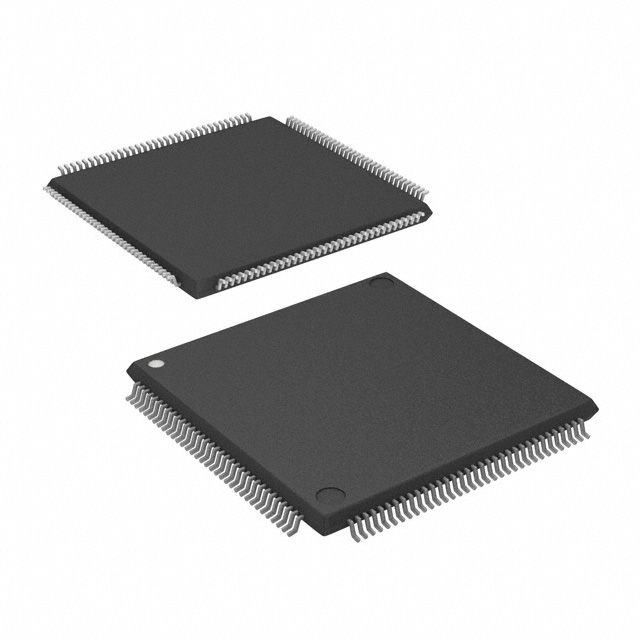
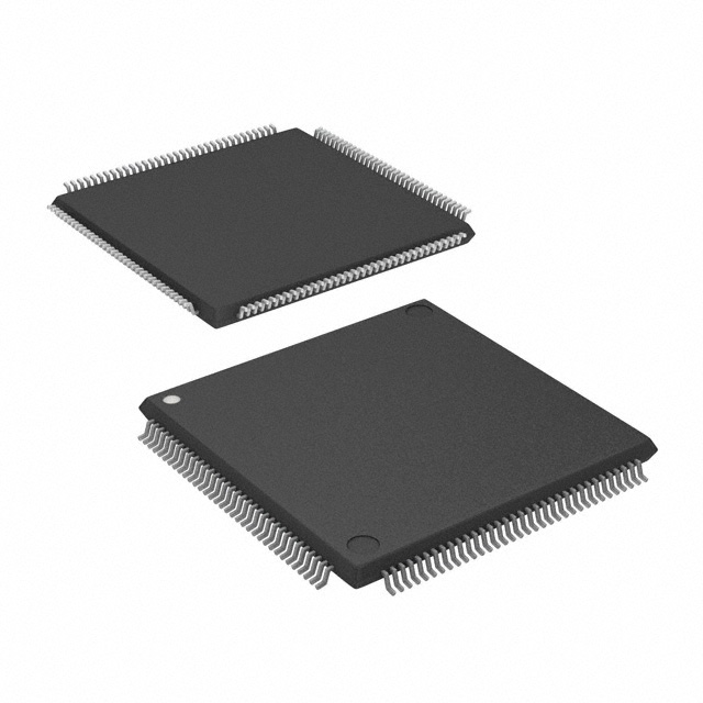
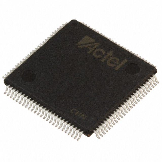
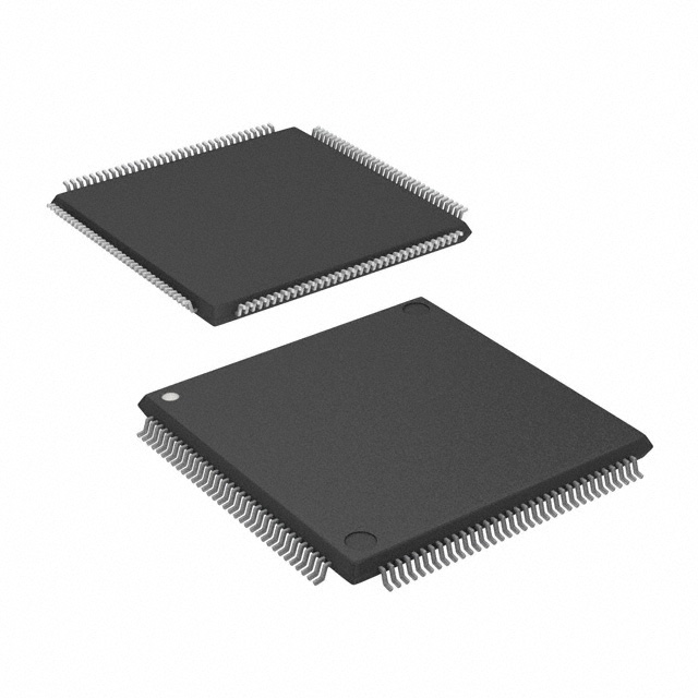
- Robust Packaging & Temperature — 100-LQFP package (supplier notes 100-TQFP, 14×14) and military-grade temperature rating from −55 °C to +125 °C.
- System Reliability & Testability — IEEE 1149.1 boundary-scan (JTAG) support and in-system diagnostic and verification capability with Silicon Explorer II.
- Security — Actel Secure Programming Technology with FuseLock™ to protect designs against reverse engineering.
- Hot-Swap & PCI Support — Hot-swap compliant I/Os and 66 MHz PCI compliance for board-level hot-insert and legacy interface applications.
Typical Applications
- Military and Rugged Embedded Systems — Military-grade temperature range and durable packaging make this FPGA suitable for mission-critical control and signal-processing tasks in harsh environments.
- Interface and Glue Logic — Configurable I/O standards and 81 user I/Os support bridging and protocol adaptation between mixed-voltage domains.
- Secure Systems and IP Protection — FuseLock secure programming and in-system diagnostic features support designs that require anti-tamper and verification capabilities.
- PCI-Capable Boards — 66 MHz PCI compliance and hot-swap I/O suitability make the device useful for PCI interface logic and hot-pluggable board subsystems.
Unique Advantages
- Nonvolatile, Single-Chip Solution: Eliminates the need for external configuration memory, simplifying BOM and system integration.
- Wide Voltage and I/O Compatibility: Supports multiple I/O standards and a broad supply range (2.25 V–5.25 V) for flexible interfacing across legacy and modern domains.
- Rugged Temperature Rating: Military-grade operation from −55 °C to +125 °C supports deployment in extreme environments.
- Deterministic Timing and Diagnostics: Series features include deterministic, user-controllable timing and in-system diagnostic support for predictable system behavior and testability.
- Security-Oriented Programming: FuseLock programming technology reduces risk of IP theft and reverse engineering.
Why Choose A54SX16A-1TQG100M?
The A54SX16A-1TQG100M positions itself as a robust, mid-capacity FPGA option for designers who need a nonvolatile, single-chip programmable logic device with military-grade reliability. With 24,000 system gates, 1,452 logic elements, and 81 configurable I/Os, it balances logic density and I/O flexibility while supporting mixed-voltage systems and hot-swap board environments.
This device is suited to development teams focused on secure, deterministic embedded designs that require extended temperature operation, JTAG testability, and series-proven features such as FuseLock secure programming and in-system diagnostics. It offers a compact package option for applications where ruggedness, IO configurability, and system-level integration matter.
Request a quote or submit an inquiry to receive pricing, availability, and ordering details for the A54SX16A-1TQG100M. Our team can assist with lead times and configuration options to support your design cycle.





















Date Founded: 1989
Headquarters: Chandler, Arizona, USA
Employees: 22,000+
Revenue: $8.349 Billion
Certifications and Memberships: ISO9001:2015, IATF16949:2016, AS 9100D




