
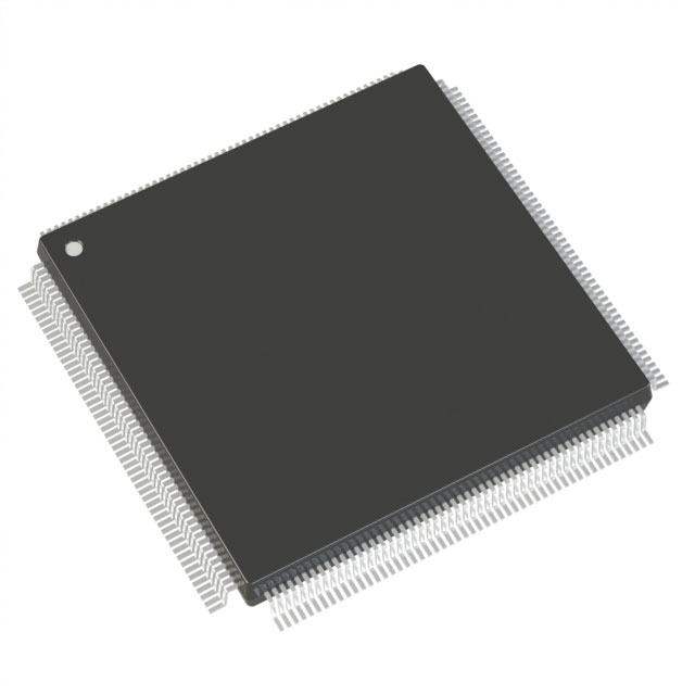
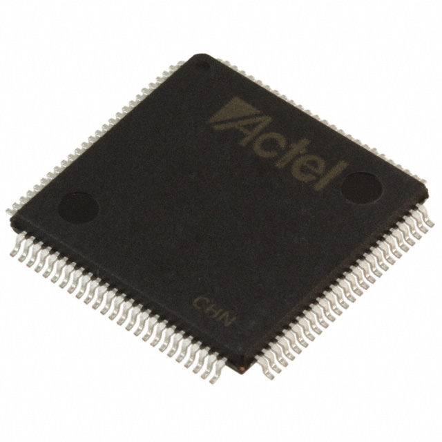
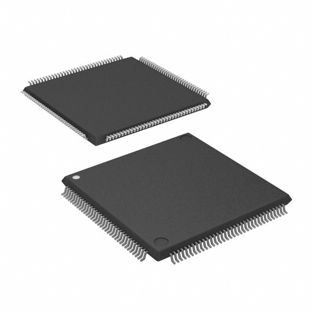
A54SX16A-2PQ208
| Part Description |
SX-A Field Programmable Gate Array (FPGA) IC 175 208-BFQFP |
|---|---|
| Quantity | 1,285 Available (as of June 18, 2026) |
| Product Category | Field Programmable Gate Array (FPGA) |
|---|---|
| Manufacturer | Microchip Technology |
| Manufacturing Status | Obsolete |
| Manufacturer Standard Lead Time | Contact Us |
| Datasheet |
Specifications & Environmental
| Device Package | 208-PQFP (28x28) | Grade | Commercial | Operating Temperature | 0°C – 70°C | ||
|---|---|---|---|---|---|---|---|
| Package / Case | 208-BFQFP | Number of I/O | 175 | Voltage | 2.25 V - 5.25 V | ||
| Mounting Method | Surface Mount | RoHS Compliance | RoHS non-compliant | REACH Compliance | REACH Unaffected | ||
| Moisture Sensitivity Level | 3 (168 Hours) | Number of LABs/CLBs | 1452 | Number of Logic Elements/Cells | 1452 | ||
| Number of Gates | 24000 | ECCN | 3A991D | HTS Code | 8542.39.0001 | ||
| Qualification | N/A |
Overview of A54SX16A-2PQ208 – SX-A Field Programmable Gate Array (FPGA) IC 175 208-BFQFP
The A54SX16A-2PQ208 is a nonvolatile SX-A family FPGA from Microchip Technology, delivering 24,000 system gates in a single-chip, programmable logic device. It provides flexible mixed-voltage I/O, hot-swap–capable interfaces and deterministic timing control suitable for system-level logic integration where on-chip security and in-system diagnostics are required.
With up to 1,452 logic elements and 175 user-programmable I/Os in a 208-pin PQFP/BFQFP package, this device targets applications that require moderate gate density, extensive I/O, and stable configuration without external volatile configuration memory.
Key Features
- Logic Capacity Approximately 24,000 system gates with 1,452 logic elements (combinatorial cells) and up to 2,012 dedicated flip-flops available within the SX-A family architecture.
- I/O Density & Flexibility 175 user-programmable I/O pins supported in the 208-pin package; configurable I/O supports 3.3 V / 5 V PCI, 5 V TTL, 3.3 V LVTTL and 2.5 V LVCMOS2 levels per the SX-A family specification.
- Mixed-Voltage Operation Supports 2.5 V, 3.3 V and 5 V mixed-voltage operation with 5 V input tolerance and 5 V drive strength as documented for the SX-A family.
- Nonvolatile Single-Chip Solution On-chip nonvolatile configuration removes the need for external configuration memory, simplifying board-level design and startup behavior.
- Power & I/O Robustness Hot-swap–compliant I/Os and power-up/power-down friendly operation with no sequencing required for supply voltages.
- Performance SX-A family performance targets listed at up to 250 MHz system performance and up to 350 MHz internal performance (family values).
- Security & Test Actel Secure Programming Technology with FuseLock™ and IEEE 1149.1 (JTAG) boundary-scan support for device security and testability.
- Package & Supply 208-pin BFQFP (supplier references 208-PQFP 28×28); voltage supply range 2.25 V to 5.25 V; commercial temperature grade 0 °C to 70 °C.
- Standards Compatibility 66 MHz PCI compliant as specified in the SX-A family datasheet.
- RoHS Compliance Device is RoHS compliant.
Typical Applications
- PCI-compliant add-on cards Use the device where 66 MHz PCI compatibility and configurable 3.3 V / 5 V I/O support are required for peripheral interfacing.
- Mixed-voltage system glue Bridge logic domains and implement interface translation in systems with 2.5 V, 3.3 V and 5 V signaling, leveraging 5 V input tolerance and configurable I/O.
- Embedded logic with secure configuration Deploy as a nonvolatile programmable logic element in embedded systems that benefit from on-chip secure programming (FuseLock™) and in-system verification capabilities.
Unique Advantages
- Single-chip nonvolatile configuration: Eliminates the need for external configuration memory, reducing BOM and simplifying board design.
- Flexible I/O voltage support: Configurable I/O standards and mixed-voltage operation enable simple interfacing across legacy and modern logic levels.
- Hot-swap and power-up robustness: Hot-swap–compliant I/Os and power-up/power-down friendly behavior reduce system sequencing complexity.
- Security and testability: FuseLock™ secure programming and IEEE 1149.1 JTAG boundary-scan improve IP protection and production test capability.
- Moderate gate density with high I/O count: 24,000 system gates and 175 I/Os in a 208-pin package balance logic capacity and connectivity for mid-range designs.
- RoHS compliant: Meets environmental restrictions for lead-free assembly and regulatory alignment.
Why Choose A54SX16A-2PQ208?
The A54SX16A-2PQ208 offers a balanced combination of moderate gate capacity, extensive I/O, and nonvolatile single-chip configuration for designs that require reliable, in-field programmable logic without external configuration devices. Its mixed-voltage I/O flexibility and hot-swap capability make it well suited to systems that integrate legacy buses or require robust power sequencing behavior.
This device is a practical choice for engineers building mid-density programmable logic solutions who need secure configuration, boundary-scan testability, and a commercial-temperature grade package with a well-documented family feature set.
Request a quote or submit an inquiry to purchase the A54SX16A-2PQ208 and confirm availability and pricing for your project needs.


Date Founded: 1989
Headquarters: Chandler, Arizona, USA
Employees: 22,000+
Revenue: $8.349 Billion
Certifications and Memberships: ISO9001:2015, IATF16949:2016, AS 9100D


