
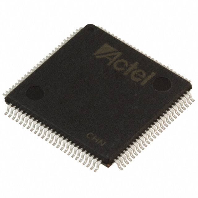
A54SX16A-2PQG208I
| Part Description |
SX-A Field Programmable Gate Array (FPGA) IC 175 208-BFQFP |
|---|---|
| Quantity | 1,072 Available (as of June 18, 2026) |

| Product Category | Field Programmable Gate Array (FPGA) |
|---|---|
| Manufacturer | Microchip Technology |
| Manufacturing Status | Active |
| Manufacturer Standard Lead Time | 14 Weeks |
| Datasheet |
Specifications & Environmental
| Device Package | 208-PQFP (28x28) | Grade | Industrial | Operating Temperature | -40°C – 85°C | ||
|---|---|---|---|---|---|---|---|
| Package / Case | 208-BFQFP | Number of I/O | 175 | Voltage | 2.25 V - 5.25 V | ||
| Mounting Method | Surface Mount | RoHS Compliance | ROHS3 Compliant | REACH Compliance | REACH Unaffected | ||
| Moisture Sensitivity Level | 3 (168 Hours) | Number of LABs/CLBs | 1452 | Number of Logic Elements/Cells | 1452 | ||
| Number of Gates | 24000 | ECCN | 3A991D | HTS Code | 8542.39.0001 | ||
| Qualification | N/A |
Overview of A54SX16A-2PQG208I – SX-A Field Programmable Gate Array (FPGA) IC 175 208-BFQFP
The A54SX16A-2PQG208I is an SX-A family field programmable gate array (FPGA) in a 208-pin BFQFP package designed for industrial embedded applications. It delivers a nonvolatile, single-chip FPGA architecture with up to approximately 24,000 system gates and 1,452 logic elements, supporting mixed-voltage I/O and deterministic timing for reliable system integration.
Built for applications requiring extensive I/O and configurable logic, this industrial-grade device supports a wide supply range and temperature operating window while providing features such as hot-swap–compliant I/Os, in-system diagnostic capability, and boundary-scan (JTAG) testing.
Key Features
- Core Performance — SX-A family performance characteristics include up to 250 MHz system performance and up to 350 MHz internal performance (family-level specifications).
- Logic Capacity — Approximately 24,000 system gates and 1,452 logic elements suitable for medium-complexity FPGA implementations.
- I/O and Interface Flexibility — 175 user-programmable I/O pins with configurable I/O support for 3.3 V / 5 V PCI, 5 V TTL, 3.3 V LVTTL, and 2.5 V LVCMOS2, enabling mixed-voltage interfacing and 5 V input tolerance with 5 V drive strength (family-level features).
- Nonvolatile Single-Chip Configuration — Nonvolatile architecture removes the need for external configuration memory and supports power-up/power-down friendly operation without sequencing requirements.
- System Integration and Test — Boundary-scan testing compliant with IEEE 1149.1 (JTAG) and in-system diagnostic/verification capability with Silicon Explorer II (family-level tools).
- Power and Voltage — Wide supply voltage range from 2.25 V to 5.25 V for flexible power-rail designs.
- Package and Mounting — Surface-mount 208-pin BFQFP (208-PQFP, 28 × 28 mm supplier package) suitable for standard PCB assembly.
- Industrial Temperature Grade — Rated for operation from –40 °C to 85 °C.
- Regulatory — RoHS compliant.
- Security — Actel Secure Programming Technology with FuseLock™ for protection against reverse engineering and design theft (family-level feature).
Typical Applications
- Industrial control and automation — Use the device’s industrial temperature rating, mixed-voltage I/O and dense I/O count to implement control logic, protocol bridging, and I/O aggregation in factory and process systems.
- Embedded system interfaces — 175 user I/Os and flexible I/O standards enable integration with sensors, peripherals and legacy logic levels in embedded platforms.
- PCI and bus bridging — Family-level support for 66 MHz PCI and configurable I/O options make the device suited for adding custom logic or protocol adaptation in PCI-based subsystems.
- Secure hardware implementations — Built-in FuseLock programming technology provides a layer of protection for proprietary logic and intellectual property.
Unique Advantages
- Highly integrated logic capacity — Approximately 24,000 system gates and 1,452 logic elements reduce the need for additional discrete logic, simplifying board-level design.
- Nonvolatile, single-chip solution — Eliminates external configuration memory and simplifies power sequencing and system start-up.
- Wide supply and I/O voltage flexibility — 2.25 V to 5.25 V supply range and multi-voltage I/O support enable interfacing with varied sub-systems without level-shifting components.
- Industrial reliability — –40 °C to 85 °C operating range and surface-mount 208-pin package suited for industrial environments.
- Built-in test and diagnostics — JTAG boundary-scan compatibility and in-system diagnostic capability streamline board bring-up and manufacturing test flows.
- IP protection — FuseLock secure programming technology helps protect design assets against reverse engineering.
Why Choose A54SX16A-2PQG208I?
The A54SX16A-2PQG208I positions itself as a robust, industrial-grade FPGA option within the SX-A family for designs needing substantial I/O, mixed-voltage interfacing and nonvolatile configuration. With approximately 24,000 gates, 1,452 logic elements, and family-level performance up to 250 MHz system operation, it provides a balance of integration and deterministic behavior for embedded and control-oriented applications.
Its single-chip nonvolatile architecture, JTAG boundary-scan support, and in-system diagnostic capabilities deliver practical advantages for manufacturing, field diagnostics and protecting intellectual property, making it well suited for engineers and procurement teams focused on dependable, compact FPGA implementations.
Request a quote or submit an inquiry to obtain pricing, availability, and lead-time information for the A54SX16A-2PQG208I.


Date Founded: 1989
Headquarters: Chandler, Arizona, USA
Employees: 22,000+
Revenue: $8.349 Billion
Certifications and Memberships: ISO9001:2015, IATF16949:2016, AS 9100D


