
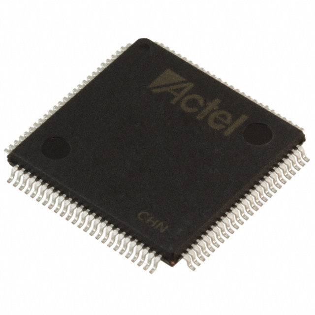
A54SX16A-2TQ100
| Part Description |
SX-A Field Programmable Gate Array (FPGA) IC 81 100-LQFP |
|---|---|
| Quantity | 379 Available (as of June 15, 2026) |
| Product Category | Field Programmable Gate Array (FPGA) |
|---|---|
| Manufacturer | Microchip Technology |
| Manufacturing Status | Obsolete |
| Manufacturer Standard Lead Time | Contact Us |
| Datasheet |
Specifications & Environmental
| Device Package | 100-TQFP (14x14) | Grade | Commercial | Operating Temperature | 0°C – 70°C | ||
|---|---|---|---|---|---|---|---|
| Package / Case | 100-LQFP | Number of I/O | 81 | Voltage | 2.25 V - 5.25 V | ||
| Mounting Method | Surface Mount | RoHS Compliance | RoHS non-compliant | REACH Compliance | REACH Unaffected | ||
| Moisture Sensitivity Level | 3 (168 Hours) | Number of LABs/CLBs | 1452 | Number of Logic Elements/Cells | 1452 | ||
| Number of Gates | 24000 | ECCN | 3A991D | HTS Code | 8542.39.0001 | ||
| Qualification | N/A |
Overview of A54SX16A-2TQ100 – SX-A FPGA, 24,000 System Gates, 100-pin TQFP
The A54SX16A-2TQ100 is a member of the SX-A family of nonvolatile field programmable gate arrays from Microchip Technology. It delivers a compact, single-chip FPGA solution with 24,000 system gates and 1,452 logic elements suitable for designs that require deterministic timing, in-system diagnostics, and mixed-voltage I/O flexibility.
Engineered for commercial-temperature embedded applications, this device targets designs that need configurable I/O standards, boundary-scan testability, and single-chip nonvolatile configuration while operating from a wide supply range.
Key Features
- Core Capacity and Logic — 24,000 system gates and 1,452 logic elements provide substantial combinatorial and sequential resources for control, glue-logic, and custom logic functions.
- Flip-Flop Resources — Up to 2,012 dedicated flip-flops for synchronous designs and state storage.
- Performance — Datasheet-level system performance up to 250 MHz and internal performance up to 350 MHz for timing-critical paths.
- I/O Count and Flexibility — 81 user I/Os with hot-swap compliant I/Os, configurable weak pull-up/pull-down at power-up, and individual output slew-rate control for signal integrity tuning.
- Mixed-Voltage and PCI Support — Configurable I/O support for 3.3 V / 5 V PCI, 5 V TTL, 3.3 V LVTTL, and 2.5 V LVCMOS2; supports 2.5 V, 3.3 V, and 5 V mixed-voltage operation with 5 V input tolerance and 5 V drive strength. Device is 66 MHz PCI compliant per datasheet.
- Nonvolatile Single-Chip Configuration — Device retains configuration without external memory, simplifying system BOM and boot behaviour.
- Security and Test — Actel Secure Programming Technology with FuseLock™ to protect designs, plus IEEE 1149.1 (JTAG) boundary-scan testing for board-level validation.
- In-System Diagnostics — Unique in-system diagnostic and verification capability with Silicon Explorer II, enabling field-level debug and verification.
- Power and Packaging — Operates from 2.25 V to 5.25 V, surface-mount mounting, available in a 100-pin thin quad flat pack (TQFP, 14×14) / 100-LQFP package case. RoHS compliant.
- Commercial Temperature Grade — Rated for 0 °C to +70 °C operation for standard commercial applications.
Typical Applications
- PCI Interface and Bus Logic — Use the device where 66 MHz PCI compliance and mixed-voltage I/O support are required to implement bus interfaces, glue logic, or protocol bridging.
- Embedded Control and Timing — Implement deterministic, timing-sensitive control logic using the device’s flip-flop resources and predictable timing characteristics.
- Field Diagnostics and Testable Systems — Leverage boundary-scan (IEEE 1149.1) and Silicon Explorer II support for in-system verification and field diagnostics.
- Compact, Nonvolatile FPGA Solutions — Deploy in systems that benefit from single-chip, nonvolatile configuration to reduce external components and simplify system boot.
Unique Advantages
- Flexible Mixed-Voltage I/O: Supports 2.5 V, 3.3 V and 5 V signaling with 5 V input tolerance, enabling straightforward interfacing to a wide range of legacy and modern peripherals.
- Nonvolatile Single-Chip Design: Eliminates the need for external configuration memory, reducing BOM complexity and improving system reliability.
- Built-in Security: FuseLock™ secure programming protects intellectual property and prevents reverse engineering of the programmed design.
- Board-Level Testability: IEEE 1149.1 boundary-scan support enables efficient board testing and manufacturing debug without additional instrumentation.
- Diagnostic Visibility: Silicon Explorer II compatibility provides a dedicated in-system diagnostic pathway for verification and troubleshooting.
- Commercial-Grade Operation: Rated for 0 °C to +70 °C with RoHS-compliant packaging and surface-mount mounting suitable for standard commercial environments.
Why Choose A54SX16A-2TQ100?
The A54SX16A-2TQ100 combines a sizeable logic capacity (24,000 system gates and 1,452 logic elements) with mixed-voltage I/O flexibility and nonvolatile single-chip configuration, making it a practical choice for commercial embedded designs that require reliable, deterministic logic and in-system diagnostic capabilities. Its support for PCI signaling, boundary-scan, and secure programming addresses common needs in interface, control, and testable system designs.
Designed for engineers who need a compact, RoHS-compliant FPGA in a 100-pin TQFP/LQFP package, this device provides a balance of integration, configurability, and testability backed by Microchip Technology’s SX-A family feature set.
Request a quote or submit a sales inquiry to discuss pricing, availability, and lead times for the A54SX16A-2TQ100.


Date Founded: 1989
Headquarters: Chandler, Arizona, USA
Employees: 22,000+
Revenue: $8.349 Billion
Certifications and Memberships: ISO9001:2015, IATF16949:2016, AS 9100D


