
A54SX16A-1TQG144M
| Part Description |
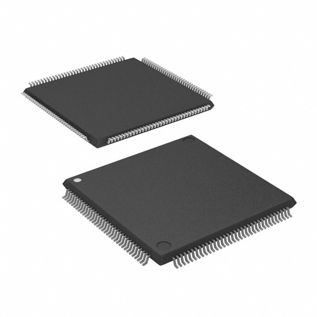
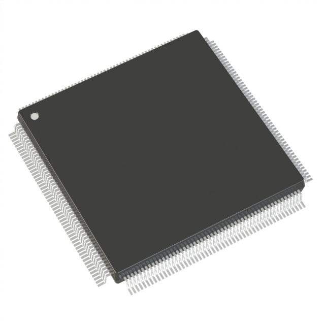
SX-A Field Programmable Gate Array (FPGA) IC 111 144-LQFP |
|---|---|
| Quantity | 635 Available (as of June 14, 2026) |
| Product Category | Field Programmable Gate Array (FPGA) |
|---|---|
| Manufacturer | Microchip Technology |
| Manufacturing Status | Active |
| Manufacturer Standard Lead Time | 20 Weeks |
| Datasheet |
Specifications & Environmental
| Device Package | 144-TQFP (20x20) | Grade | Military | Operating Temperature | -55°C – 125°C | ||
|---|---|---|---|---|---|---|---|
| Package / Case | 144-LQFP | Number of I/O | 111 | Voltage | 2.25 V - 5.25 V | ||
| Mounting Method | Surface Mount | RoHS Compliance | ROHS3 Compliant | REACH Compliance | REACH Unaffected | ||
| Moisture Sensitivity Level | 3 (168 Hours) | Number of LABs/CLBs | 1452 | Number of Logic Elements/Cells | 1452 | ||
| Number of Gates | 24000 | ECCN | 3A001A2C | HTS Code | 8542.39.0001 | ||
| Qualification | N/A |
Overview of A54SX16A-1TQG144M – SX-A Field Programmable Gate Array (FPGA) IC 111 144-LQFP
The A54SX16A-1TQG144M is a SX‑A family Field Programmable Gate Array (FPGA) from Microchip Technology, supplied in a 144-pin LQFP/TQFP surface-mount package. It provides approximately 24,000 system gates implemented across 1,452 logic elements with 111 user I/Os, targeting applications that require nonvolatile FPGA functionality with military temperature capability.
Built on the SX‑A architecture, this device delivers family-level features such as nonvolatile single‑chip configuration, deterministic timing, and in‑system diagnostics aimed at designs requiring secure programming and robust I/O control across mixed-voltage environments.
Key Features
- Core Capacity 1,452 logic elements and approximately 24,000 system gates to implement control, glue logic, and medium-complexity digital functions.
- User I/O 111 programmable user I/Os with configurable I/O support for 3.3 V / 5 V PCI, 5 V TTL, 3.3 V LVTTL and 2.5 V LVCMOS2 levels, plus 5 V input tolerance and 5 V drive strength options.
- Performance Family-level performance indicators include up to 250 MHz system performance and up to 350 MHz internal performance (SX‑A family specifications).
- Nonvolatile, Single‑Chip Configuration Single‑chip nonvolatile architecture eliminates separate configuration memory and supports power‑up/power‑down friendly operation without sequencing.
- Security & Programming Actel Secure Programming Technology with FuseLock™ for IP protection and in‑system programming capabilities.
- Testability & Diagnostics Boundary-scan testing compliant with IEEE 1149.1 (JTAG) and unique in‑system diagnostic/verification capability with Silicon Explorer II (SX‑A family feature).
- I/O Control Hot‑swap compliant I/Os, configurable weak pull‑up/pull‑down at power‑up, and individual output slew‑rate control for signal integrity management.
- Power & Voltage Wide supply range from 2.25 V to 5.25 V to support mixed-voltage systems and flexible board-level integration.
- Package & Mounting 144‑pin LQFP package (supplier device package: 144‑TQFP 20×20) in a surface-mount form factor for compact PCB layouts.
- Environmental & Reliability Military grade device with operating temperature range from −55°C to +125°C and RoHS compliance.
Typical Applications
- Military and aerospace systems Use in defense electronics and avionics where military temperature range and ruggedized packaging are required for reliable operation.
- PCI and bus interface logic Implement PCI-compliant glue logic and interface bridging leveraging configurable I/O and 66 MHz PCI support from the SX‑A family.
- Secure embedded control On-chip nonvolatile configuration and FuseLock™ security support protected programmable logic in secure systems.
- In-system test and diagnostics Leverage boundary-scan (JTAG) and SX‑A in‑system diagnostic features for board-level testability and field diagnostics.
Unique Advantages
- Highly integrated logic capacity: 1,452 logic elements and ~24,000 system gates reduce external glue logic and simplify board design.
- Nonvolatile single‑chip solution: Eliminates the need for external configuration memory and simplifies power sequencing on the board.
- Mixed-voltage flexibility: 2.25 V to 5.25 V supply range with configurable I/O standards and 5 V tolerance supports diverse system voltage domains.
- Designed for harsh environments: Military-grade temperature rating (−55°C to +125°C) enables deployment in demanding thermal conditions.
- Built-in security and diagnostics: FuseLock™ programming and in‑system diagnostic capabilities enhance IP protection and facilitate verification and maintenance.
- Test and integration friendly: IEEE 1149.1 boundary-scan support and configurable I/O features streamline production test and board bring-up.
Why Choose A54SX16A-1TQG144M?
The A54SX16A-1TQG144M positions itself as a robust, nonvolatile FPGA option within the SX‑A family that balances moderate logic capacity with comprehensive I/O configurability and military-rated environmental capability. It is suited to designs that require secure, deterministic programmable logic in a compact 144‑pin surface-mount package.
Designers seeking a field-programmable device with family-proven features—such as in‑system diagnostics, boundary-scan testing, configurable I/O standards, and FuseLock™ security—will find this device aligned with applications that demand reliable operation across mixed-voltage domains and extreme temperatures.
Request a quote or submit an inquiry to purchase the A54SX16A-1TQG144M for your next design. Provide part number and quantity to begin the quoting process.


Date Founded: 1989
Headquarters: Chandler, Arizona, USA
Employees: 22,000+
Revenue: $8.349 Billion
Certifications and Memberships: ISO9001:2015, IATF16949:2016, AS 9100D


