
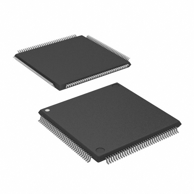
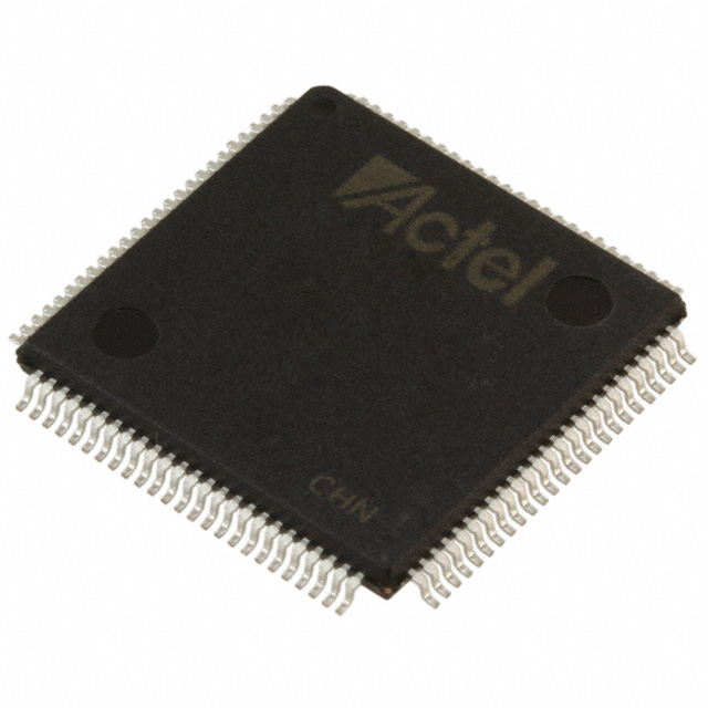
A54SX16A-1TQG144
| Part Description |
SX-A Field Programmable Gate Array (FPGA) IC 113 144-LQFP |
|---|---|
| Quantity | 671 Available (as of October 8, 2026) |
| Product Category | Field Programmable Gate Array (FPGA) |
|---|---|
| Manufacturer | Microchip Technology |
| Manufacturing Status | Active |
| Manufacturer Standard Lead Time | 12 Weeks |
| Datasheet |
Specifications & Environmental
| Device Package | 144-TQFP (20x20) | Grade | Commercial | Operating Temperature | 0°C – 70°C | ||
|---|---|---|---|---|---|---|---|
| Package / Case | 144-LQFP | Number of I/O | 113 | Voltage | 2.25 V - 5.25 V | ||
| Mounting Method | Surface Mount | RoHS Compliance | ROHS3 Compliant | REACH Compliance | REACH Unaffected | ||
| Moisture Sensitivity Level | 3 (168 Hours) | Number of LABs/CLBs | 1452 | Number of Logic Elements/Cells | 1452 | ||
| Number of Gates | 24000 | ECCN | 3A991D | HTS Code | 8542.39.0001 | ||
| Qualification | N/A |
Overview of A54SX16A-1TQG144 – SX-A Field Programmable Gate Array (FPGA) IC 113 144-LQFP
The A54SX16A-1TQG144 is a commercial-grade, nonvolatile SX-A family FPGA from Microchip Technology. It delivers 24,000 system gates implemented across 1,452 logic elements with 113 user I/Os in a 144-pin LQFP/TQFP surface-mount package.
Designed for mixed-voltage embedded applications, the device supports a wide supply range (2.25 V to 5.25 V), provides in-system programmability and diagnostic capabilities, and inherits SX-A family characteristics such as hot-swap compliant I/Os and boundary-scan (JTAG) support.
Key Features
- Core Capacity — 24,000 system gates implemented as approximately 1,452 logic elements, suitable for glue logic, control glue, and medium-complexity FPGA functions.
- User I/O — 113 user-programmable I/Os with configurable I/O support for multiple signaling standards and 5 V input tolerance per SX-A family specifications.
- Nonvolatile Single-Chip Architecture — SX-A family single-chip, nonvolatile configuration that enables in-system programming and retains configuration without external memory.
- Voltage Flexibility — Supported supply range from 2.25 V to 5.25 V, enabling mixed-voltage system designs and interfacing with legacy 5 V logic.
- No Embedded RAM — Total RAM bits: 0, indicating the device is optimized for logic and flip‑flop based functions rather than distributed on-chip memory.
- Performance and Timing — SX-A family performance characteristics include up to 250 MHz system performance and up to 350 MHz internal performance, along with deterministic, user-controllable timing.
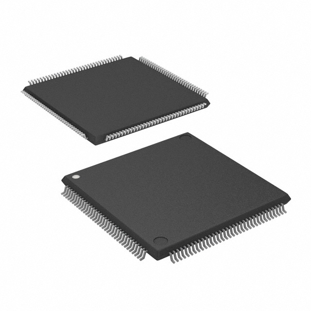
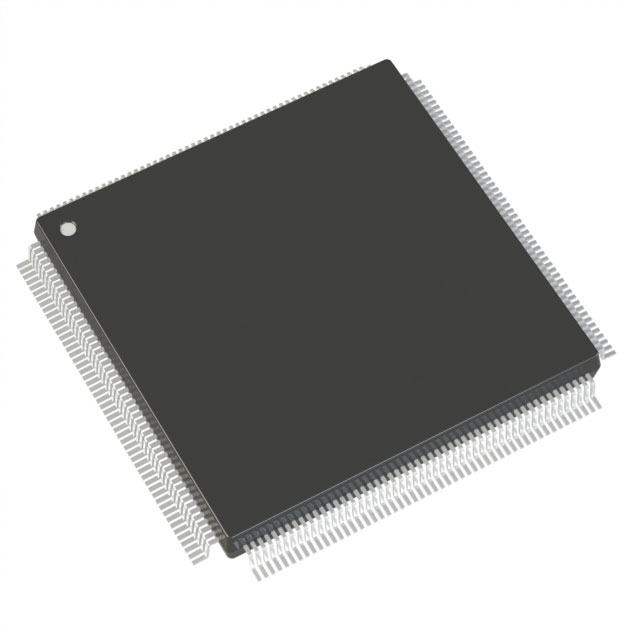
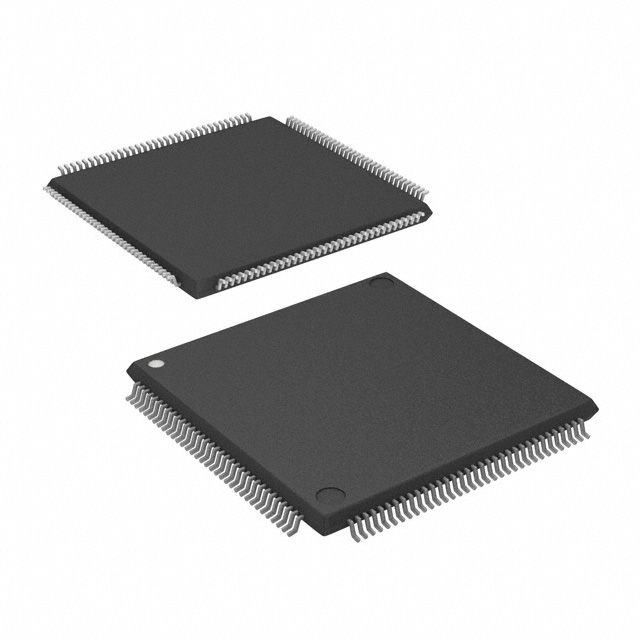
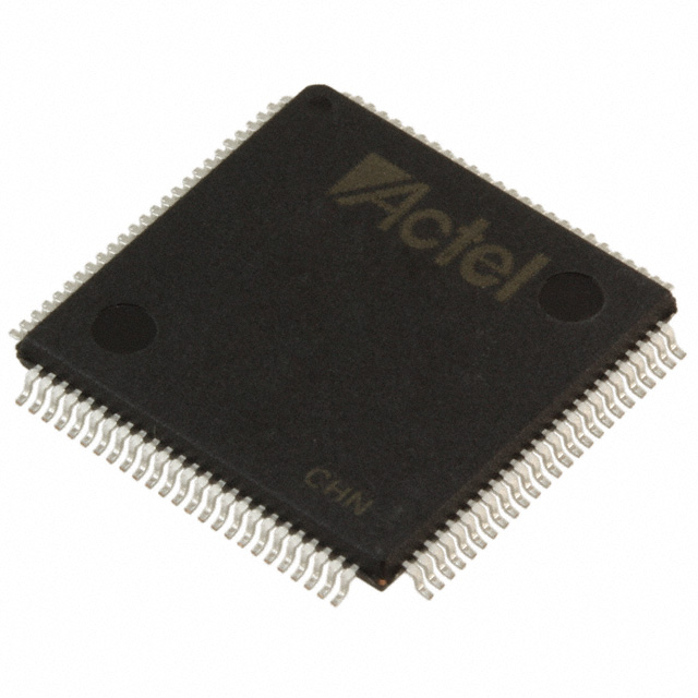
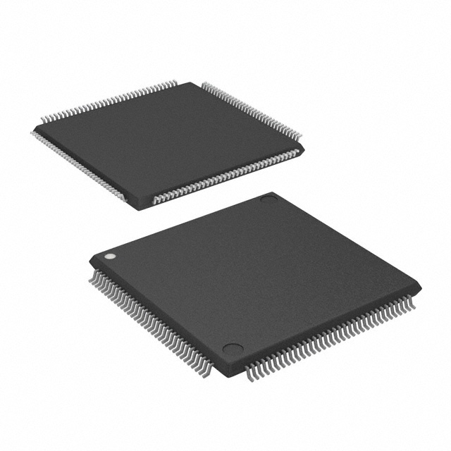
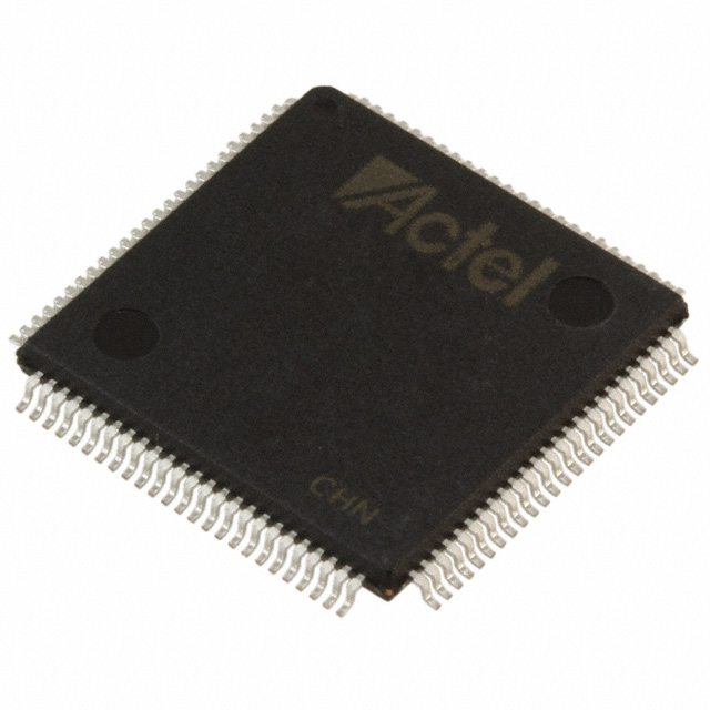
- Packaging & Mounting — 144-pin LQFP package case (supplier device package listed as 144-TQFP, 20×20); surface-mount mounting for board-level assembly.
- Reliability & Test — Boundary-scan testing (IEEE 1149.1/JTAG) support and family-level features such as power-up/down friendly behavior and configurable weak pull-up/pull-down on I/Os at power-up.
- Regulatory — RoHS-compliant.
- Operating Conditions — Commercial temperature grade with operating range 0 °C to 70 °C.
Typical Applications
- Mixed-Voltage Interface and Glue Logic — Use the device to bridge and interface between 5 V legacy logic and lower-voltage domains thanks to its wide supply range and 5 V input tolerance.
- PCI and Legacy Bus Adaptation — The SX-A family includes 66 MHz PCI compliance; this device can be applied where medium-speed PCI-compliant logic adaptation or buffering is required.
- Embedded Control and State Machines — Compact footprint and nonvolatile configuration make the device suitable for board-level control functions, protocol translation, and state-machine implementations.
- In-System Diagnostics & Production Test — Boundary-scan (JTAG) and family diagnostic capabilities support manufacturing test, in-system verification, and field diagnostics.
Unique Advantages
- Compact, Gate-Level Integration: 24,000 system gates and 1,452 logic elements deliver a mid-range integration point that reduces external glue components and simplifies board-level design.
- Mixed-Voltage Compatibility: Broad supply range (2.25 V–5.25 V) and configurable I/Os allow direct interfacing across multiple logic families, reducing level-shifter requirements.
- Nonvolatile Configuration: Single-chip nonvolatile architecture removes the need for external configuration memory and streamlines power-up behavior.
- Deterministic Timing and Testability: Family features such as user-controllable timing, JTAG boundary-scan, and in-system diagnostics improve system validation and maintainability.
- Surface-Mount Package for Compact Designs: 144-pin LQFP/TQFP surface-mount package enables a smaller PCB footprint while providing a generous I/O count for mid-complexity applications.
- RoHS-Compliant: Compliant with RoHS directives for lead-free manufacturing and environmental responsibility.
Why Choose A54SX16A-1TQG144?
The A54SX16A-1TQG144 positions as a practical, mid-capacity FPGA choice for commercial-temperature embedded systems that require nonvolatile configuration, mixed-voltage I/O flexibility, and reliable board-level testability. With 24,000 system gates and 1,452 logic elements, it targets designs that need moderate logic density without external configuration memory.
Engineers designing protocol adapters, glue logic, bus interfaces or embedded control functions will find the device’s voltage range, I/O count, JTAG support and compact 144-pin package useful for reducing BOM complexity and simplifying integration. As part of the SX-A family, it benefits from family-level performance and diagnostic features documented in the SX-A datasheet.
Request a quote or submit an inquiry to purchase the A54SX16A-1TQG144 and receive pricing and availability information for your project requirements.





















Date Founded: 1989
Headquarters: Chandler, Arizona, USA
Employees: 22,000+
Revenue: $8.349 Billion
Certifications and Memberships: ISO9001:2015, IATF16949:2016, AS 9100D




