
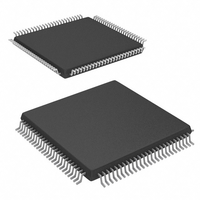
A54SX16P-1PQG208M
| Part Description |
SX Field Programmable Gate Array (FPGA) IC 175 208-BFQFP |
|---|---|
| Quantity | 1,339 Available (as of June 15, 2026) |

| Product Category | Field Programmable Gate Array (FPGA) |
|---|---|
| Manufacturer | Microchip Technology |
| Manufacturing Status | Active |
| Manufacturer Standard Lead Time | 20 Weeks |
| Datasheet |
Specifications & Environmental
| Device Package | 208-PQFP (28x28) | Grade | Military | Operating Temperature | -55°C – 125°C | ||
|---|---|---|---|---|---|---|---|
| Package / Case | 208-BFQFP | Number of I/O | 175 | Voltage | 3 V - 5.5 V | ||
| Mounting Method | Surface Mount | RoHS Compliance | ROHS3 Compliant | REACH Compliance | REACH Unaffected | ||
| Moisture Sensitivity Level | 3 (168 Hours) | Number of LABs/CLBs | 1452 | Number of Logic Elements/Cells | 1452 | ||
| Number of Gates | 24000 | ECCN | 3A001A2C | HTS Code | 8542.39.0001 | ||
| Qualification | N/A |
Overview of A54SX16P-1PQG208M – SX Field Programmable Gate Array (FPGA) IC 175 208-BFQFP
The A54SX16P-1PQG208M is a nonvolatile SX-series FPGA offering approximately 24,000 system gates and 1,452 logic elements in a 208-pin BFQFP package. Designed for mixed-voltage systems, it supports 3 V to 5.5 V supplies and up to 175 user I/Os, providing flexible I/O configuration and reliable operation across a wide temperature range.
This military-grade device is optimized for applications requiring deterministic timing, in-system diagnostics, and secure programming, backed by features such as hot-swap–capable I/Os, JTAG boundary-scan, and Actel/ Microchip secure programming technology.
Key Features
- Core Capacity Approximately 24,000 system gates and 1,452 logic elements for mid-density logic integration.
- Performance -1 speed grade available (approximately 15% faster than standard), with SX-family performance characteristics documented up to 250 MHz system and 350 MHz internal operation in the family datasheet.
- I/O and Mixed-Voltage Support 175 user-programmable I/Os with configurable support for multiple voltage standards; compatible with 3.3 V/5 V PCI and mixed 2.5 V, 3.3 V, and 5 V I/O environments.
- Nonvolatile, Single-Chip Solution Built-in nonvolatile configuration—single-chip FPGA eliminates the need for external configuration memory.
- System and Test Support Boundary-scan (IEEE 1149.1 JTAG) for board-level testability and in-system diagnostic capabilities with Silicon Explorer II diagnostics noted for the SX family.
- Security Actel Secure Programming Technology with FuseLock™ provides protection against reverse engineering and design theft (family feature).
- Power and I/O Robustness Hot-swap–compliant I/Os and power-up/power-down friendly behavior (no sequencing required for supply voltages).
- Package and Mounting 208-BFQFP (supplier package 208-PQFP, 28 × 28 mm), surface-mount device suitable for standard PCB assembly.
- Temperature and Grade Military grade with an operating temperature range of −55 °C to +125 °C for high-reliability deployments.
- Environmental Compliance RoHS compliant.
Typical Applications
- Aerospace & Defense Military-grade operating temperature and robust packaging make this FPGA suitable for avionics, rugged communications, and other defense electronics requiring reliability across extreme environments.
- Mixed-Voltage System Interfaces Configurable I/Os and 5 V input tolerance enable integration with legacy 5 V logic, PCI interfaces, and modern 2.5 V/3.3 V subsystems.
- Secure or Sensitive Designs On-chip secure programming (FuseLock) and single-chip nonvolatile configuration help protect IP in applications where reverse-engineering risks must be mitigated.
- In-System Diagnostic and Test Solutions JTAG boundary-scan and the SX family’s in-system diagnostic capabilities support board-level testing, fault isolation, and field diagnostics.
Unique Advantages
- Deterministic, Controllable Timing: Family-level support for deterministic timing simplifies system timing closure and design verification.
- Single-Chip Nonvolatile Design: Eliminates external configuration components and simplifies BOM and board-level design.
- Wide Supply Range: 3 V to 5.5 V supply capability accommodates a variety of legacy and modern system voltage domains.
- High-Reliability Temperature Rating: −55 °C to +125 °C operating range and military grade classification for deployment in demanding environments.
- Comprehensive Test and Security Features: Boundary-scan (IEEE 1149.1) and secure programming technology reduce manufacturing risk and protect IP.
- Flexible, High-Density I/O: 175 user I/Os enable dense peripheral and interface routing in a 208-pin package.
Why Choose A54SX16P-1PQG208M?
The A54SX16P-1PQG208M positions itself as a robust, mid-density FPGA solution for designs that require nonvolatile configuration, mixed-voltage interfacing, and military-grade environmental tolerance. Its combination of roughly 24,000 system gates, 1,452 logic elements, and 175 user I/Os provides designers the integration needed to consolidate logic, reduce board-level complexity, and maintain secure, in-field programmability.
Choose this device for projects that demand deterministic timing, board-level testability, and protection of intellectual property, while benefiting from a single-chip FPGA architecture and wide operating voltage and temperature ranges.
Request a quote or submit an inquiry to obtain pricing, availability, and lead-time information for the A54SX16P-1PQG208M.


Date Founded: 1989
Headquarters: Chandler, Arizona, USA
Employees: 22,000+
Revenue: $8.349 Billion
Certifications and Memberships: ISO9001:2015, IATF16949:2016, AS 9100D


