
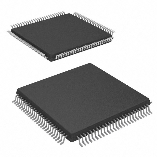
A54SX16P-1VQ100
| Part Description |
SX Field Programmable Gate Array (FPGA) IC 81 100-TQFP |
|---|---|
| Quantity | 1,292 Available (as of June 17, 2026) |

| Product Category | Field Programmable Gate Array (FPGA) |
|---|---|
| Manufacturer | Microchip Technology |
| Manufacturing Status | Obsolete |
| Manufacturer Standard Lead Time | Contact Us |
| Datasheet |
Specifications & Environmental
| Device Package | 100-VQFP (14x14) | Grade | Commercial | Operating Temperature | 0°C – 70°C | ||
|---|---|---|---|---|---|---|---|
| Package / Case | 100-TQFP | Number of I/O | 81 | Voltage | 3 V - 5.25 V | ||
| Mounting Method | Surface Mount | RoHS Compliance | RoHS non-compliant | REACH Compliance | REACH Unaffected | ||
| Moisture Sensitivity Level | 3 (168 Hours) | Number of LABs/CLBs | 1452 | Number of Logic Elements/Cells | 1452 | ||
| Number of Gates | 24000 | ECCN | 3A991D | HTS Code | 8542.39.0001 | ||
| Qualification | N/A |
Overview of A54SX16P-1VQ100 – SX Field Programmable Gate Array (FPGA) IC 81 100-TQFP
The A54SX16P-1VQ100 is a commercial-grade SX-A family FPGA from Microchip Technology in a 100-pin thin quad flat pack (TQFP) surface-mount package. It provides 24,000 system gates implemented as approximately 1,452 logic elements with 81 user I/Os, making it suitable for compact, reprogrammable digital logic, interface control, and system integration tasks in commercial embedded designs.
As a member of the SX-A family, this device benefits from single-chip nonvolatile configuration and a set of system features aimed at deterministic timing, in-system diagnostics, and flexible I/O voltage support.
Key Features
- Logic Capacity Approximately 24,000 system gates implemented as 1,452 logic elements, enabling moderate-density logic integration in a compact package.
- User I/O 81 user-programmable I/O pins provided in the 100-TQFP package for signal interfacing and peripheral connections.
- Package & Mounting 100-pin TQFP (14 × 14 mm) surface-mount package (supplier device package 100-VQFP), optimized for compact board layouts.
- Voltage Support Wide supply range from 3.0 V to 5.25 V; SX-A family supports mixed-voltage operation including 2.5 V, 3.3 V and 5 V I/O levels with 5 V input tolerance and 5 V drive strength (family-level capability).
- Speed Grade This part carries the –1 speed grade designation (approximately 15% faster than standard for SX-A family parts).
- Commercial Temperature Rated for commercial operation from 0 °C to 70 °C.
- Nonvolatile Single-Chip Configuration SX-A family devices are provided as nonvolatile, single-chip solutions for retained configuration without external configuration memory (family-level feature).
- System & Test Features Family features include boundary-scan testing compliant with IEEE 1149.1 (JTAG), in-system diagnostic and verification capability, and configurable I/O behavior at power-up.
- Regulatory RoHS compliant.
Typical Applications
- Commercial Embedded Systems Use the A54SX16P-1VQ100 for compact embedded control and logic tasks where moderate gate density and a 100-TQFP footprint are required.
- Interface Control & Glue Logic Implement protocol adaptation, bus bridging, and glue logic leveraging 81 I/Os and mixed-voltage I/O capability.
- PCI-Enabled Designs Leverage SX-A family support for 66 MHz PCI signaling for interface and peripheral bridging in commercial systems.
- In-System Diagnostics & Boundary Scan Integrate JTAG boundary-scan and family diagnostics to simplify testing and bring-up of board-level designs.
Unique Advantages
- Compact, Moderate-Density FPGA Delivers ~24k system gates and 1,452 logic elements in a 100-pin TQFP, reducing board area while providing useful logic capacity.
- Flexible I/O Voltage Options Family-level support for mixed 2.5 V / 3.3 V / 5 V operation and 5 V tolerance simplifies interfacing to a wide range of legacy and modern peripherals.
- Nonvolatile, Single-Chip Solution Eliminates the need for external configuration memory and simplifies system power-up behavior.
- Deterministic Timing & Diagnostics SX-A family features deliver predictable timing behavior and in-system diagnostic capabilities to shorten development and validation cycles.
- Testability IEEE 1149.1 (JTAG) boundary-scan support eases board-level testing and manufacturing diagnostics.
- RoHS Compliant Meets lead-free and restricted-substances requirements for commercial deployments.
Why Choose A54SX16P-1VQ100?
The A54SX16P-1VQ100 strikes a balance between logic capacity, I/O count, and package size for commercial embedded applications that require a nonvolatile, reprogrammable logic device in a compact TQFP footprint. With approximately 1,452 logic elements, 81 user I/Os, and SX-A family system features—such as boundary-scan, in-system diagnostics, and mixed-voltage I/O capability—this device is well suited for designers building interface controllers, glue logic, and moderate-density digital subsystems.
Its –1 speed grade and family-provided system features support projects that need a modest performance uplift and robust test/diagnostic options without external configuration components. RoHS compliance and surface-mount packaging make it appropriate for commercial product assemblies.
Request a quote or submit an inquiry to receive pricing and availability information for the A54SX16P-1VQ100.


Date Founded: 1989
Headquarters: Chandler, Arizona, USA
Employees: 22,000+
Revenue: $8.349 Billion
Certifications and Memberships: ISO9001:2015, IATF16949:2016, AS 9100D


