
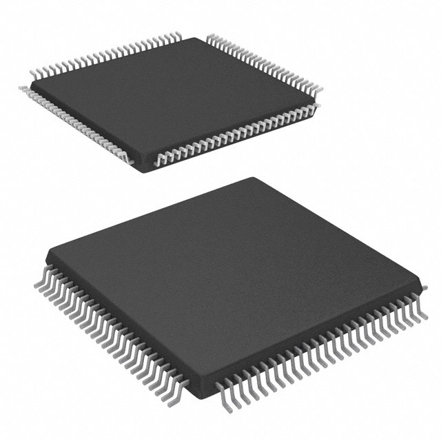
A54SX16P-2VQ100
| Part Description |
SX Field Programmable Gate Array (FPGA) IC 81 100-TQFP |
|---|---|
| Quantity | 320 Available (as of June 10, 2026) |

| Product Category | Field Programmable Gate Array (FPGA) |
|---|---|
| Manufacturer | Microchip Technology |
| Manufacturing Status | Obsolete |
| Manufacturer Standard Lead Time | Contact Us |
| Datasheet |
Specifications & Environmental
| Device Package | 100-VQFP (14x14) | Grade | Commercial | Operating Temperature | 0°C – 70°C | ||
|---|---|---|---|---|---|---|---|
| Package / Case | 100-TQFP | Number of I/O | 81 | Voltage | 3 V - 5.25 V | ||
| Mounting Method | Surface Mount | RoHS Compliance | RoHS non-compliant | REACH Compliance | REACH Unaffected | ||
| Moisture Sensitivity Level | 3 (168 Hours) | Number of LABs/CLBs | 1452 | Number of Logic Elements/Cells | 1452 | ||
| Number of Gates | 24000 | ECCN | 3A991D | HTS Code | 8542.39.0001 | ||
| Qualification | N/A |
Overview of A54SX16P-2VQ100 – SX Field Programmable Gate Array (FPGA) IC 81 I/O, 100-TQFP
The A54SX16P-2VQ100 is a commercial-grade SX family FPGA offered by Microchip Technology. It is a nonvolatile, single-chip FPGA optimized for mixed-voltage I/O designs and compact board footprints, supplied in a 100-pin thin quad flat pack (100-TQFP / 14×14 VQFP footprint). Typical system-level performance and configurable I/O support make it suitable for interface logic, protocol bridging, and in-system verification tasks.
Key device resources include approximately 24,000 system gates, 1,452 logic elements, and 81 user I/O pins. The device is designed for 3.0–5.25 V supply environments and is rated for commercial temperature operation (0 °C to +70 °C).
Key Features
- Core Capacity — Approximately 24,000 system gates and 1,452 logic elements provide a mid-range logic resource for glue logic, protocol conversion, and control functions.
- User I/O — 81 user-programmable I/O pins in the 100-TQFP package, configurable for multiple voltage standards to support mixed-voltage systems.
- Mixed-Voltage I/O Support — Configurable I/O for 3.3 V/5 V PCI, 5 V TTL, 3.3 V LVTTL, and 2.5 V LVCMOS2; supports 2.5 V, 3.3 V, and 5 V operation with 5 V input tolerance and 5 V drive strength.
- Performance — Series datasheet specifies up to 250 MHz system performance and up to 350 MHz internal performance for timing-critical logic.
- Nonvolatile Single-Chip Solution — Maintains configuration without external volatile configuration memory, simplifying system design and boot behavior.
- Power and Robustness — Power-up/down friendly operation with no required supply sequencing and hot-swap compliant I/Os for robust board-level integration.
- Security and Test — On-device secure programming technology (FuseLock™) to prevent reverse engineering and IEEE 1149.1 (JTAG) boundary-scan testing for board-level diagnostics.
- Package and Mounting — 100-TQFP surface-mount package (supplier package: 100-VQFP, 14×14) for compact PCB designs.
- Environmental — RoHS compliant; rated for commercial temperature range 0 °C to +70 °C.
- On-Chip Memory — No embedded RAM bits (Total RAM bits: 0), suitable for designs that rely on external memory or logic-only implementations.
Typical Applications
- PCI and Interface Logic — 66 MHz PCI compliance and flexible I/O standards make the device suitable for protocol bridging and bus interface functions.
- Mixed-Voltage System Glue — Configurable I/O voltages and 5 V tolerance support level translation and interfacing between legacy and modern logic domains.
- In-System Diagnostics and Verification — JTAG boundary-scan support and in-system diagnostic capability enable board-level testing and functional verification.
- Secure Logic Functions — On-device FuseLock™ programming provides protection for intellectual property and configuration security in fielded products.
Unique Advantages
- Nonvolatile Configuration — Eliminates the need for external configuration memory, reducing BOM complexity and improving system boot reliability.
- Flexible Mixed-Voltage I/O — Broad I/O standard support and 5 V tolerance simplify integration with diverse peripherals and legacy interfaces.
- Compact Package — 100-TQFP footprint offers a space-efficient solution for constrained PCB real estate while providing 81 user I/Os.
- Design Security — Built-in FuseLock™ secure programming helps protect designs from reverse engineering and unauthorized access.
- Testability — IEEE 1149.1 boundary-scan support enables streamlined board-level testing and reduces development time for manufacturing test.
- Robust Power Handling — Power-up/down friendly operation with hot-swap compliant I/Os lowers system integration risk and simplifies power sequencing.
Why Choose A54SX16P-2VQ100?
The A54SX16P-2VQ100 delivers a balanced combination of mid-range logic capacity, mixed-voltage I/O flexibility, and nonvolatile configuration in a compact 100-TQFP package. Its commercial temperature rating and RoHS compliance make it appropriate for a wide range of board-level logic and interface tasks where embedded RAM is not required.
This device is a practical choice for engineers seeking a secure, testable FPGA solution for protocol bridging, interface logic, and mixed-voltage system designs that benefit from nonvolatile configuration and robust I/O behavior.
Request a quote or submit an inquiry to get pricing and availability for the A54SX16P-2VQ100.


Date Founded: 1989
Headquarters: Chandler, Arizona, USA
Employees: 22,000+
Revenue: $8.349 Billion
Certifications and Memberships: ISO9001:2015, IATF16949:2016, AS 9100D


