
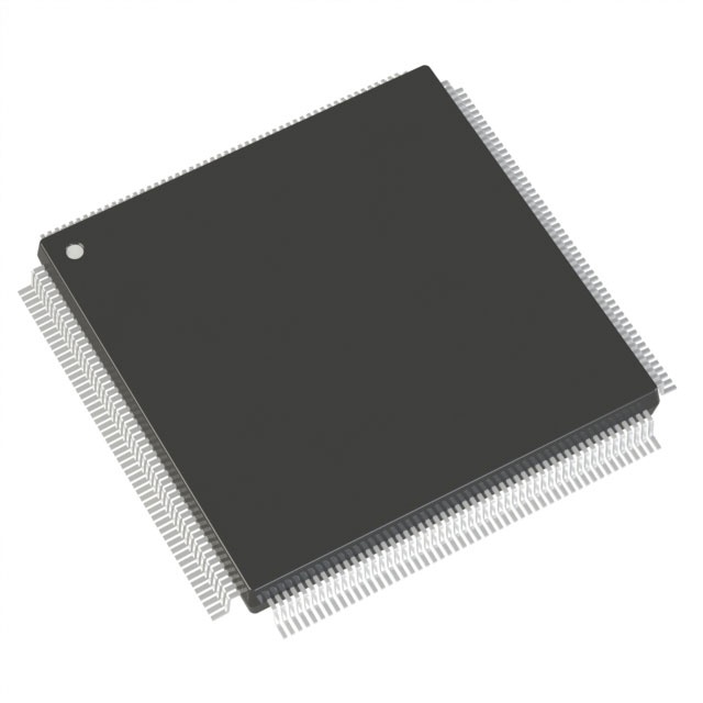
A54SX16P-PQ208
| Part Description |
SX Field Programmable Gate Array (FPGA) IC 175 208-BFQFP |
|---|---|
| Quantity | 1,868 Available (as of June 10, 2026) |
| Product Category | Field Programmable Gate Array (FPGA) |
|---|---|
| Manufacturer | Microchip Technology |
| Manufacturing Status | Obsolete |
| Manufacturer Standard Lead Time | Contact Us |
| Datasheet |
Specifications & Environmental
| Device Package | 208-PQFP (28x28) | Grade | Commercial | Operating Temperature | 0°C – 70°C | ||
|---|---|---|---|---|---|---|---|
| Package / Case | 208-BFQFP | Number of I/O | 175 | Voltage | 3 V - 5.25 V | ||
| Mounting Method | Surface Mount | RoHS Compliance | RoHS non-compliant | REACH Compliance | REACH Unaffected | ||
| Moisture Sensitivity Level | 3 (168 Hours) | Number of LABs/CLBs | 1452 | Number of Logic Elements/Cells | 1452 | ||
| Number of Gates | 24000 | ECCN | 3A991D | HTS Code | 8542.39.0001 | ||
| Qualification | N/A |
Overview of A54SX16P-PQ208 – SX Field Programmable Gate Array (FPGA) IC 175 208-BFQFP
The A54SX16P-PQ208 is a nonvolatile SX-A family FPGA provided in a 208-pin BFQFP/PQFP package. It delivers a compact programmable logic solution with 24,000 system gates and 1,452 logic elements, and supports 175 user I/Os for flexible interface and glue-logic applications.
Designed for commercial embedded designs, the device operates from a 3 V to 5.25 V supply and across a 0 °C to 70 °C commercial temperature range, and includes series-level features such as deterministic timing, in-system diagnostics, and secure programming options.
Key Features
- Core Performance — SX-A family performance characteristics including up to 250 MHz system performance and up to 350 MHz internal performance as specified for the family.
- Logic Capacity — 24,000 system gates and approximately 1,452 logic elements to implement control, glue logic, and medium-density custom logic functions.
- User I/O — 175 user-programmable I/Os with configurable I/O options. I/Os support mixed-voltage operation and 5 V input tolerance as defined for the SX-A family.
- Memory — Total on-chip RAM bits: 0 (no embedded RAM).
- Power and Voltage — Operates from 3 V to 5.25 V supply. Family-level support for mixed 2.5 V, 3.3 V, and 5 V I/O operation and 5 V drive strength.
- Package & Mounting — 208-pin BFQFP / PQFP package (supplier device package 208-PQFP 28 × 28), surface-mount mounting type, RoHS compliant.
- System Reliability & Test — Boundary-scan testing compliant with IEEE 1149.1 (JTAG) and in-system diagnostic/verification capability available through family tools.
- Power-Up/Down Friendly — Family-level support for no required sequencing of supply voltages; hot-swap compliant I/Os and configurable weak pull-up or pull-down at power-up.
- Security & Control — Family-provided secure programming technology and selectable output slew-rate control for signal integrity management.
- Grade — Commercial grade device with operating temperature from 0 °C to 70 °C.
Typical Applications
- PCI interface and bridge logic — Family support for 66 MHz PCI and configurable 3.3 V/5 V PCI I/O makes the device suitable for PCI glue logic and interface bridging.
- Custom I/O aggregation — High I/O count and mixed-voltage support enable aggregation and translation of multiple peripheral interfaces in compact systems.
- In-system diagnostics and verification — Built-in support for in-system diagnostic tools and JTAG boundary-scan facilitates hardware bring-up and board-level testing.
- Hot-swap and power-sequencing-sensitive designs — Hot-swap compliant I/Os and power-up/down friendly behavior reduce system-level power sequencing constraints.
Unique Advantages
- Nonvolatile single-chip solution: Eliminates the need for external configuration memory and simplifies board-level design.
- Flexible mixed-voltage I/O: Configurable I/O levels and 5 V input tolerance support interfacing to a wide range of legacy and modern peripherals.
- Deterministic, user-controllable timing: Family-level deterministic timing features help meet timing closure and predictable system behavior.
- High I/O density in a standard package: 175 user I/Os in a 208-pin PQFP/BFQFP footprint enable compact integration without large BGA packages.
- Integrated test and security features: Boundary-scan (IEEE 1149.1), in-system diagnostics, and secure programming technology provide testability and IP protection.
- RoHS compliant: Meets lead-free environmental requirements for commercial electronics manufacturing.
Why Choose A54SX16P-PQ208?
The A54SX16P-PQ208 combines a moderate logic capacity (24,000 system gates / 1,452 logic elements) with a high user I/O count and family-level performance characteristics to address embedded designs requiring flexible I/O, deterministic timing, and nonvolatile configuration. Its surface-mount 208-pin PQFP/BFQFP package and commercial temperature grade make it suitable for compact, production-oriented electronics.
Designers who need in-system diagnostic capability, JTAG boundary-scan, and secure programming options will find the device’s family features useful for validation, test, and IP protection while maintaining a straightforward board-level integration profile.
Request a quote or submit an inquiry to check availability, pricing, and lead times for the A54SX16P-PQ208.


Date Founded: 1989
Headquarters: Chandler, Arizona, USA
Employees: 22,000+
Revenue: $8.349 Billion
Certifications and Memberships: ISO9001:2015, IATF16949:2016, AS 9100D


