
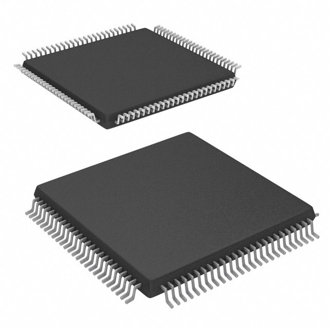
A54SX16P-2VQG100
| Part Description |
SX Field Programmable Gate Array (FPGA) IC 81 100-TQFP |
|---|---|
| Quantity | 938 Available (as of June 15, 2026) |

| Product Category | Field Programmable Gate Array (FPGA) |
|---|---|
| Manufacturer | Microchip Technology |
| Manufacturing Status | Active |
| Manufacturer Standard Lead Time | 52 Weeks |
| Datasheet |
Specifications & Environmental
| Device Package | 100-VQFP (14x14) | Grade | Commercial | Operating Temperature | 0°C – 70°C | ||
|---|---|---|---|---|---|---|---|
| Package / Case | 100-TQFP | Number of I/O | 81 | Voltage | 3 V - 5.25 V | ||
| Mounting Method | Surface Mount | RoHS Compliance | ROHS3 Compliant | REACH Compliance | REACH Unaffected | ||
| Moisture Sensitivity Level | 3 (168 Hours) | Number of LABs/CLBs | 1452 | Number of Logic Elements/Cells | 1452 | ||
| Number of Gates | 24000 | ECCN | 3A991D | HTS Code | 8542.39.0001 | ||
| Qualification | N/A |
Overview of A54SX16P-2VQG100 – SX Field Programmable Gate Array (FPGA) IC 81 100-TQFP
The A54SX16P-2VQG100 is a nonvolatile SX-A family FPGA provided in a 100-pin TQFP surface-mount package. It delivers a mid-range integration point with 24,000 system gates and 1,452 logic elements, and is aimed at designers needing a single-chip, reconfigurable logic solution with flexible I/O and deterministic timing.
Designed for commercial applications, the device supports mixed-voltage operation and configurable I/O standards, making it suitable for embedded control, interface bridging, and PCI-compatible systems where in-system diagnostics, security and reliable power-up behavior are important.
Key Features
- Core Capacity — 24,000 system gates and 1,452 logic elements provide a compact, deterministic logic resource pool for glue logic, control tasks and moderate-complexity functions.
- User I/O — 81 user-programmable I/O pins in the 100‑TQFP package with configurable I/O support for 3.3 V/5 V PCI, 5 V TTL, 3.3 V LVTTL and 2.5 V LVCMOS2 standards.
- Performance — Family-level performance targets include up to 250 MHz system performance and up to 350 MHz internal performance for timing-critical paths.
- Voltage & Mixed-Voltage Operation — 3 V to 5.25 V supply range with support for 2.5 V, 3.3 V and 5 V mixed-voltage operation; includes 5 V input tolerance and 5 V drive strength where applicable.
- Package & Mounting — Surface-mount 100-TQFP (14 × 14 mm supplier package) for compact board designs.
- Commercial Grade & Temperature — Commercial grade device rated for 0 °C to 70 °C operation.
- Power and I/O Robustness — Hot-swap compliant I/Os and power-up/down friendly behavior that requires no supply sequencing.
- Design-for-Test & Security — Boundary-scan testing (IEEE 1149.1 JTAG) and Actel Secure Programming Technology with FuseLock for protection of programmed designs.
- In-System Diagnostics & Deterministic Timing — Supports in-system diagnostic and verification capability (Silicon Explorer II) and user-controllable, deterministic timing; enables up to 100% resource utilization and pin locking.
- Environmental Compliance — RoHS compliant.
Typical Applications
- PCI-based systems — 66 MHz PCI compliance and configurable 3.3 V/5 V PCI I/O support make the device appropriate for add-in cards and host interface logic.
- Embedded control and glue logic — Mid-range gate count and 1,452 logic elements suit control, protocol adaptation, and board-level glue in compact systems.
- Mixed-voltage interfacing — Mixed-voltage operation and 5 V tolerant I/Os enable direct interfacing between legacy 5 V peripherals and modern 3.3/2.5 V logic without external translators.
- Production test & in-system verification — JTAG boundary-scan and Silicon Explorer II diagnostic capability streamline manufacturing test and field verification.
- Hot-swap and power-sensitive designs — Hot-swap compliant I/Os and power-up/-down friendly behavior reduce board-level sequencing constraints in systems that require live insertion or variable power domains.
Unique Advantages
- Nonvolatile single-chip solution: Eliminates the need for external configuration memory, simplifying board design and startup sequencing.
- Flexible mixed-voltage I/O: Direct support for 5 V, 3.3 V and 2.5 V interface standards reduces BOM and eases integration with a range of peripherals.
- Deterministic resources: 1,452 logic elements and deterministic, user-controllable timing help achieve predictable behavior in control and timing-sensitive applications.
- Built-in security and test features: FuseLock programming and JTAG boundary-scan enhance IP protection and production testability.
- Production and field diagnostics: In-system diagnostic support (Silicon Explorer II) accelerates bring-up, debugging and fault isolation.
- Commercial-grade, RoHS-compliant packaging: 100‑TQFP surface-mount package provides a compact form factor that meets RoHS environmental requirements.
Why Choose A54SX16P-2VQG100?
The A54SX16P-2VQG100 occupies a mid-range position within the SX-A FPGA family, combining a nonvolatile single-chip architecture with 24,000 system gates, 1,452 logic elements and 81 user I/Os. It is suited to designers who need a compact, reconfigurable device with mixed-voltage I/O capability, predictable timing behavior and integrated test/security features.
Its commercial temperature rating, hot-swap compliant I/Os, and support for in-system diagnostics and JTAG boundary-scan make it a practical choice for embedded systems, PCI-interface logic and production-tested designs where reducing external components and simplifying bring-up are priorities.
Request a quote or contact sales to discuss availability, pricing and how the A54SX16P-2VQG100 can fit into your next design project.


Date Founded: 1989
Headquarters: Chandler, Arizona, USA
Employees: 22,000+
Revenue: $8.349 Billion
Certifications and Memberships: ISO9001:2015, IATF16949:2016, AS 9100D


