
A54SX16P-VQG100
| Part Description |
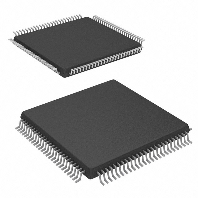
SX Field Programmable Gate Array (FPGA) IC 81 100-TQFP |
|---|---|
| Quantity | 1,063 Available (as of June 15, 2026) |

| Product Category | Field Programmable Gate Array (FPGA) |
|---|---|
| Manufacturer | Microchip Technology |
| Manufacturing Status | Active |
| Manufacturer Standard Lead Time | 52 Weeks |
| Datasheet |
Specifications & Environmental
| Device Package | 100-VQFP (14x14) | Grade | Commercial | Operating Temperature | 0°C – 70°C | ||
|---|---|---|---|---|---|---|---|
| Package / Case | 100-TQFP | Number of I/O | 81 | Voltage | 3 V - 5.25 V | ||
| Mounting Method | Surface Mount | RoHS Compliance | ROHS3 Compliant | REACH Compliance | REACH Unaffected | ||
| Moisture Sensitivity Level | 3 (168 Hours) | Number of LABs/CLBs | 1452 | Number of Logic Elements/Cells | 1452 | ||
| Number of Gates | 24000 | ECCN | 3A991D | HTS Code | 8542.39.0001 | ||
| Qualification | N/A |
Overview of A54SX16P-VQG100 – SX Field Programmable Gate Array (FPGA) IC 81 100-TQFP
The A54SX16P-VQG100 is a commercial-grade SX family FPGA supplied in a 100-pin TQFP/VQFP package and designed for surface-mount applications. It provides approximately 24,000 system gates mapped to about 1,452 logic elements and offers 81 user I/Os for compact, reprogrammable logic implementations.
As part of the SX-A family, the device inherits family-level capabilities such as nonvolatile single-chip configuration, configurable I/O voltage support, and on-board features for in-system diagnostics and boundary-scan testing—making it suitable for commercial electronic systems that require flexible mixed-voltage interfacing and secure programmable logic.
Key Features
- Logic Capacity — Approximately 24,000 system gates implemented across about 1,452 logic elements for mid-range programmable logic tasks.
- User I/O — 81 user-programmable I/O pins enabling diverse I/O requirements in a compact 100-pin TQFP package.
- Package & Mounting — 100-TQFP (supplier package: 100-VQFP, 14×14) for low-profile surface-mount PCB designs.
- Voltage Flexibility — Supports a 3 V to 5.25 V supply range and family-level configurable I/O options for multiple logic standards, enabling mixed-voltage system interfacing.
- Commercial Temperature Grade — Rated for operation from 0 °C to 70 °C for standard commercial applications.
- Nonvolatile, Single-Chip Configuration — SX-A family capability for single-chip nonvolatile configuration simplifies system boot and removes the need for external configuration memory.
- No Embedded SRAM — Total on-chip RAM bits: 0; architecture focused on configurable logic and I/O rather than embedded RAM.
- Design-for-Test and Security — Family features include boundary-scan testing (IEEE 1149.1/JTAG) and Actel Secure Programming Technology with FuseLock for design protection and in-system verification tools such as Silicon Explorer II.
- Standards & Performance (Family) — SX-A family specifications include PCI support and deterministic timing; refer to family documentation for detailed performance and speed-grade options.
- RoHS Compliant — Device is RoHS compliant for reduced environmental impact.
Typical Applications
- Commercial Embedded Systems — Implement custom logic, protocol bridging, or control functions where a commercial-temperature FPGA with modest gate and I/O counts is required.
- Mixed-Voltage Interface Design — Use configurable I/O support to bridge and interface components operating across 2.5 V, 3.3 V, and 5 V domains.
- PCI and Bus Interface Logic — Leverage family-level PCI compliance for bus-interface glue logic and custom peripheral implementations in PCI-based platforms.
- In-System Diagnostics & Prototyping — Utilize the SX family’s in-system diagnostic and verification capabilities for board-level debugging and production validation.
Unique Advantages
- Right-sized Logic for Mid-range Designs: Approximately 24,000 gates and ~1,452 logic elements provide a balance of capacity and cost for commercial applications.
- Compact, Surface-Mount Packaging: 100-TQFP/VQFP packaging with 81 I/Os enables dense PCB layouts while maintaining ample external connectivity.
- Flexible Supply and I/O Voltage Range: 3 V to 5.25 V operation and family-configurable I/O standards simplify integration into mixed-voltage systems.
- Nonvolatile Single-Chip Solution: Eliminates the need for external configuration memory, reducing BOM and simplifying system boot flow.
- Testability and Security Built In: Boundary-scan (JTAG) support and FuseLock secure programming help protect IP and support production test flows.
- RoHS Compliance: Environmentally compliant manufacturing for commercial product lines.
Why Choose A54SX16P-VQG100?
The A54SX16P-VQG100 targets commercial applications that need a compact, nonvolatile FPGA with mid-range logic capacity and a modest but versatile I/O count. Its 100-pin TQFP package and surface-mount form factor make it a practical choice for space-constrained boards, while the 3 V–5.25 V supply range and configurable I/O support ease integration into systems with mixed-voltage components.
By combining approximately 24,000 gates, about 1,452 logic elements, secure programming features, and family-level diagnostic support, this device offers a pragmatic balance of integration, security, and testability for designers building commercial electronic products.
Request a quote or contact sales for pricing and availability of the A54SX16P-VQG100.


Date Founded: 1989
Headquarters: Chandler, Arizona, USA
Employees: 22,000+
Revenue: $8.349 Billion
Certifications and Memberships: ISO9001:2015, IATF16949:2016, AS 9100D


