
A54SX32-1BG329I
| Part Description |
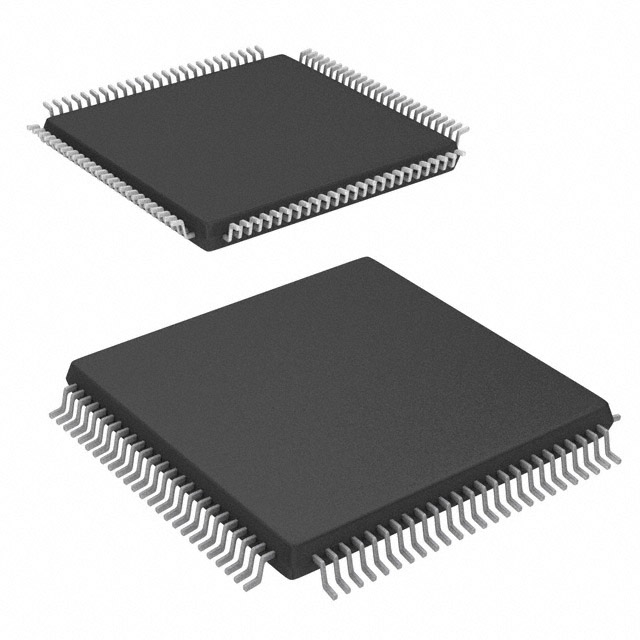
SX Field Programmable Gate Array (FPGA) IC 249 329-BBGA |
|---|---|
| Quantity | 493 Available (as of June 15, 2026) |

| Product Category | Field Programmable Gate Array (FPGA) |
|---|---|
| Manufacturer | Microchip Technology |
| Manufacturing Status | Active |
| Manufacturer Standard Lead Time | 20 Weeks |
| Datasheet |
Specifications & Environmental
| Device Package | 329-PBGA (31x31) | Grade | Industrial | Operating Temperature | -40°C – 85°C | ||
|---|---|---|---|---|---|---|---|
| Package / Case | 329-BBGA | Number of I/O | 249 | Voltage | 3 V - 5.5 V | ||
| Mounting Method | Surface Mount | RoHS Compliance | RoHS non-compliant | REACH Compliance | REACH Unaffected | ||
| Moisture Sensitivity Level | 3 (168 Hours) | Number of LABs/CLBs | 2880 | Number of Logic Elements/Cells | 2880 | ||
| Number of Gates | 48000 | ECCN | 3A991D | HTS Code | 8542.39.0001 | ||
| Qualification | N/A |
Overview of A54SX32-1BG329I – SX Field Programmable Gate Array (FPGA) IC 249 329-BBGA
The A54SX32-1BG329I is an industrial-grade SX family FPGA from Microchip Technology designed for deterministic logic implementation in compact, surface-mount form factors. It provides a balance of logic capacity, high I/O density and configurable mixed-voltage I/O to support control, interface and protocol tasks in industrial and embedded systems.
This device targets applications that require up to 48,000 system gates and 249 user I/Os in a 329-ball BGA package, offering nonvolatile single‑chip configuration and a broad operating voltage and temperature window for reliable deployment in industrial environments.
Key Features
- Logic Capacity — 48,000 system gates and 2,880 logic elements provide the resources to implement medium-complexity state machines, glue logic and protocol acceleration.
- I/O and Mixed-Voltage Support — 249 user-programmable I/Os with configurable support for 3.3 V / 5 V PCI, 5 V TTL, 3.3 V LVTTL and 2.5 V LVCMOS2; supports mixed-voltage operation with 5 V input tolerance and 5 V drive strength.
- Performance — Family-level performance specifications include up to 250 MHz system performance and up to 350 MHz internal performance for timing-critical paths.
- Nonvolatile Single-Chip Configuration — Built-in nonvolatile configuration reduces external components needed for device configuration at power-up.
- Power and I/O Robustness — Hot-swap compliant I/Os and power‑up/power‑down friendly operation with no supply sequencing required simplify board-level power management.
- Test and Debug — Boundary-scan testing compliant with IEEE 1149.1 (JTAG) and in-system diagnostic capability with Silicon Explorer II.
- Security — Actel Secure Programming Technology with FuseLock™ provides protection against reverse engineering and unauthorized readback.
- Package and Mounting — 329-ball BGA (329-BBGA / supplier package 329-PBGA 31×31) in a surface-mount package for high-density PCB designs.
- Industrial Temperature and Supply Range — Rated for industrial temperature operation (−40 °C to 85 °C) with supply range listed at 3 V to 5.5 V.
Typical Applications
- Industrial Control — Implement programmable state machines, timing logic and I/O aggregation for factory automation and motion control systems.
- Interface Bridging — Use high I/O count and mixed-voltage support to bridge disparate interfaces and implement protocol conversion between 2.5 V, 3.3 V and 5 V domains.
- Embedded System Glue Logic — Offload glue logic, reset sequencing, and custom peripheral control to a single nonvolatile FPGA to reduce BOM count.
- Test & Diagnostic Hardware — Leverage boundary-scan and in-system diagnostics for board-level validation and field troubleshooting.
Unique Advantages
- High I/O Density: 249 user I/Os provide extensive external connectivity without resorting to larger, more expensive packages.
- Flexible Voltage Interfacing: Configurable I/O standards and mixed-voltage operation simplify integration with legacy 5 V logic and modern lower-voltage peripherals.
- Nonvolatile Configuration: Single‑chip nonvolatile storage removes the need for external configuration memory and simplifies system boot.
- Industrial Ready: Specified operation from −40 °C to 85 °C and surface-mount BGA packaging support deployment in industrial environments.
- Security and Testability: FuseLock programming protection and IEEE‑1149.1 boundary-scan support help protect IP and streamline manufacturing test.
- Deterministic Timing: User-controllable timing resources enable predictable performance for time-critical designs.
Why Choose A54SX32-1BG329I?
The A54SX32-1BG329I combines a mid-range logic capacity with high I/O count and robust mixed-voltage support, making it well suited for embedded and industrial applications that require deterministic behavior, in-system debug and secure configuration. Its nonvolatile single-chip architecture and BGA packaging reduce system complexity and PCB area while supporting industrial temperature operation.
This device is appropriate for engineers and procurement teams seeking a compact, industrial-grade FPGA solution for interface control, glue logic consolidation, and board-level testability where mixed-voltage interoperablity and secure configuration are important.
Request a quote or submit an inquiry to get pricing, availability and technical support for the A54SX32-1BG329I.


Date Founded: 1989
Headquarters: Chandler, Arizona, USA
Employees: 22,000+
Revenue: $8.349 Billion
Certifications and Memberships: ISO9001:2015, IATF16949:2016, AS 9100D


