
A54SX16P-VQG100M
| Part Description |
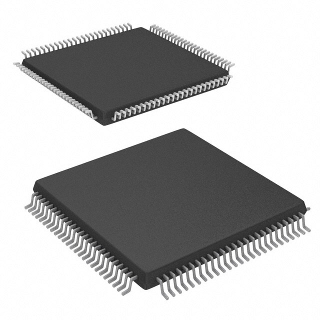
SX Field Programmable Gate Array (FPGA) IC 81 100-TQFP |
|---|---|
| Quantity | 274 Available (as of June 15, 2026) |

| Product Category | Field Programmable Gate Array (FPGA) |
|---|---|
| Manufacturer | Microchip Technology |
| Manufacturing Status | Active |
| Manufacturer Standard Lead Time | 52 Weeks |
| Datasheet |
Specifications & Environmental
| Device Package | 100-VQFP (14x14) | Grade | Military | Operating Temperature | -55°C – 125°C | ||
|---|---|---|---|---|---|---|---|
| Package / Case | 100-TQFP | Number of I/O | 81 | Voltage | 3 V - 5.5 V | ||
| Mounting Method | Surface Mount | RoHS Compliance | ROHS3 Compliant | REACH Compliance | REACH Unaffected | ||
| Moisture Sensitivity Level | 3 (168 Hours) | Number of LABs/CLBs | 1452 | Number of Logic Elements/Cells | 1452 | ||
| Number of Gates | 24000 | ECCN | 3A001A2C | HTS Code | 8542.39.0001 | ||
| Qualification | N/A |
Overview of A54SX16P-VQG100M – SX Field Programmable Gate Array (FPGA) IC 81 100-TQFP
The A54SX16P-VQG100M is a military-grade SX-A family FPGA from Microchip Technology supplied in a 100-pin thin quad flat pack (100-TQFP / 100-VQFP). It provides a nonvolatile, single-chip FPGA solution with 24,000 system gates and 1,452 logic elements suitable for high-reliability designs that require wide temperature and voltage range operation.
Designed for applications that demand secure, deterministic logic and I/O behavior, this device combines industry-oriented features—such as hot-swap-capable I/Os, configurable multi-voltage I/O support and in-system diagnostic capabilities—with a military temperature rating for deployment in harsh environments.
Key Features
- Core Capacity — 24,000 system gates with 1,452 logic elements (combinatorial/logic cells) to implement moderate-complexity digital functions.
- I/O Count & Configurability — 81 user I/O pins with configurable I/O support for 3.3 V / 5 V PCI, 5 V TTL, 3.3 V LVTTL and 2.5 V LVCMOS2; supports 5 V input tolerance and 5 V drive strength where applicable.
- Nonvolatile Single-Chip Architecture — Device retains configuration across power cycles (nonvolatile), eliminating the need for external configuration memory.
- Performance — Series-level performance indicators include up to 250 MHz system performance and up to 350 MHz internal performance (SX-A family specifications).
- Power and I/O Robustness — Hot-swap compliant I/Os and power-up/power-down friendly operation requiring no sequencing of supply voltages (SX-A family feature set).
- Security & Test — Includes Actel Secure Programming Technology with FuseLock™ to protect design IP and supports IEEE 1149.1 boundary-scan (JTAG) for board-level testing.
- Diagnostics — In-system diagnostic and verification capability available via the SX-A family Silicon Explorer II toolchain (family-level feature).
- Package & Mounting — 100-pin TQFP / VQFP (14 × 14 mm) surface-mount package suitable for board-level integration; RoHS compliant.
- Voltage & Temperature — Wide supply range from 3 V to 5.5 V and military operating temperature range of −55 °C to 125 °C.
Typical Applications
- Military and Aerospace Systems — Military-grade temperature rating and single-chip nonvolatile configuration make the part suitable for rugged, long-life deployments requiring wide temperature operation.
- PCI and Legacy Interface Designs — Configurable I/O supports 66 MHz PCI signaling and multiple logic voltage standards for bridging and interface control.
- Secure IP and Protected Designs — FuseLock™ secure programming technology helps protect intellectual property in systems that require in-field security.
- Embedded Control and Instrumentation — Deterministic, user-controllable timing and on-chip logic resources enable real-time control, protocol handling and sensor/interface glue logic.
Unique Advantages
- Nonvolatile, single-chip solution: Eliminates external configuration memory and simplifies board power sequencing and BOM.
- Wide voltage flexibility: Supports mixed 2.5 V, 3.3 V and 5 V operation with 5 V input tolerance, enabling easy interfacing to a variety of legacy and modern logic families.
- Military temperature rating: Rated for −55 °C to 125 °C, providing robustness for harsh-environment applications.
- Built-in security and testability: FuseLock™ secure programming and IEEE 1149.1 JTAG boundary-scan support aid both IP protection and manufacturing test.
- In-system diagnostics: Family-level diagnostic tools and verification capabilities streamline development and troubleshooting on deployed systems.
- Compact, industry-standard package: 100-pin TQFP/VQFP offers a compact surface-mount form factor for size-constrained boards.
Why Choose A54SX16P-VQG100M?
The A54SX16P-VQG100M positions itself as a rugged, secure and compact FPGA option within the SX-A family—offering 24,000 system gates and 1,452 logic elements in a 100-pin TQFP package with wide supply and temperature ranges. It is well suited to designers who need a nonvolatile, deterministic FPGA with configurable multi-voltage I/O and built-in security and test features for high-reliability applications.
Choose this device when your design requires a balance of moderate logic capacity, secure nonvolatile configuration, JTAG testability and military-grade environmental performance backed by the SX-A family feature set and documentation.
Request a quote or submit an inquiry to check pricing and availability for the A54SX16P-VQG100M and to discuss how its specifications match your project requirements.


Date Founded: 1989
Headquarters: Chandler, Arizona, USA
Employees: 22,000+
Revenue: $8.349 Billion
Certifications and Memberships: ISO9001:2015, IATF16949:2016, AS 9100D


