
A54SX32-BG329I
| Part Description |
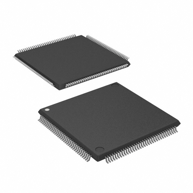
SX Field Programmable Gate Array (FPGA) IC 249 329-BBGA |
|---|---|
| Quantity | 496 Available (as of June 15, 2026) |

| Product Category | Field Programmable Gate Array (FPGA) |
|---|---|
| Manufacturer | Microchip Technology |
| Manufacturing Status | Active |
| Manufacturer Standard Lead Time | 20 Weeks |
| Datasheet |
Specifications & Environmental
| Device Package | 329-PBGA (31x31) | Grade | Industrial | Operating Temperature | -40°C – 85°C | ||
|---|---|---|---|---|---|---|---|
| Package / Case | 329-BBGA | Number of I/O | 249 | Voltage | 3 V - 5.5 V | ||
| Mounting Method | Surface Mount | RoHS Compliance | RoHS non-compliant | REACH Compliance | REACH Unaffected | ||
| Moisture Sensitivity Level | 3 (168 Hours) | Number of LABs/CLBs | 2880 | Number of Logic Elements/Cells | 2880 | ||
| Number of Gates | 48000 | ECCN | 3A991D | HTS Code | 8542.39.0001 | ||
| Qualification | N/A |
Overview of A54SX32-BG329I – SX Field Programmable Gate Array (FPGA) IC 249 329-BBGA
The A54SX32-BG329I is an SX-A family FPGA in a 329-ball BGA package, offering a nonvolatile, single-chip FPGA solution for industrial designs. Built for mixed-voltage I/O and in-system programmability, this device provides a compact, reprogrammable platform with 2,880 logic elements (approx. 48,000 system gates) and up to 249 user I/Os for complex glue logic, bus interfacing and control functions.
Designed for industrial temperature operation (–40 °C to 85 °C) and RoHS-compliant packaging, the A54SX32-BG329I targets embedded and industrial systems that require deterministic timing, configurable I/O standards, and in-system verification capabilities.
Key Features
- Core Capacity — Approximately 48,000 system gates implemented as 2,880 logic elements, suitable for mid-density logic integration and custom control functions.
- I/O Density & Flexibility — Up to 249 user I/Os with configurable support for 3.3 V / 5 V PCI, 5 V TTL, 3.3 V LVTTL and 2.5 V LVCMOS2; supports mixed-voltage operation and 5 V input tolerance.
- Performance — Series-level performance metrics include up to 250 MHz system performance and 350 MHz internal performance (as specified for the SX-A family).
- Nonvolatile, Single-Chip Solution — Single-chip, nonvolatile architecture provides in-system programmability without external configuration memory.
- Package & Mounting — 329-ball BGA (supplier device package: 329-PBGA, 31×31) in a surface-mount form factor optimized for compact board designs.
- Power & Voltage — Wide supply tolerance from 3 V to 5.5 V and power-up/power-down friendly operation (no sequencing required for supply voltages as described in the series datasheet).
- Industrial Temperature Grade — Rated for industrial operation between –40 °C and 85 °C.
- System Reliability & Test — Boundary-scan (IEEE 1149.1) for board-level testability and unique in-system diagnostic/verification capability with Silicon Explorer II.
- Security — Series-level Actel Secure Programming Technology with FuseLock™ to protect bitstream confidentiality and prevent reverse engineering.
- Regulatory — RoHS compliant packaging.
Typical Applications
- Industrial Control and Automation — Implement custom control logic, I/O aggregation and deterministic timing functions for factory automation and process control within the industrial temperature range.
- PCI and Bus Interface Logic — Support for 3.3 V/5 V PCI signaling and hot-swap compliant I/Os makes the device suitable for PCI-compliant interface logic and bridge functions.
- Mixed-Voltage I/O Systems — Use as programmable I/O adapters or protocol translators where 2.5 V, 3.3 V and 5 V mixed-voltage support and 5 V tolerance are required.
- In-System Programmable Glue Logic — Compact, nonvolatile FPGA for board-level glue logic, timing control, and configurable peripheral handling with in-system verification.
Unique Advantages
- High-density, deterministic logic: 2,880 logic elements (≈48,000 system gates) provide ample mid-range integration with predictable timing behavior.
- Flexible I/O standards: Configurable I/O supports multiple voltage standards and mixed-voltage operation to simplify interfacing with legacy and modern peripherals.
- Nonvolatile, single-chip architecture: Eliminates external configuration memory and simplifies board-level design and power sequencing.
- Industrial readiness: Specified for –40 °C to 85 °C operation and supplied in a compact 329-BBGA package for reliable deployment in industrial environments.
- Built-in test and security: Boundary-scan support and FuseLock secure programming reduce development risk and protect intellectual property.
- Broad supply tolerance: 3 V to 5.5 V supply range supports flexible power architectures and mixed-voltage systems.
Why Choose A54SX32-BG329I?
The A54SX32-BG329I provides a balanced mid-density FPGA option for industrial embedded systems that need a nonvolatile, in-system programmable device with flexible mixed-voltage I/O and a compact BGA footprint. With 2,880 logic elements, up to 249 user I/Os, and industrial temperature capability, it addresses applications requiring reliable glue logic, interface control and deterministic timing.
Backed by Microchip Technology’s SX-A family architecture, the device combines secure programming, boundary-scan testability and configurable I/O to reduce BOM complexity and streamline board-level integration for long-lived industrial deployments.
Request a quote or submit an inquiry to receive pricing and availability information for the A54SX32-BG329I. Provide part number and required quantity to expedite your response.


Date Founded: 1989
Headquarters: Chandler, Arizona, USA
Employees: 22,000+
Revenue: $8.349 Billion
Certifications and Memberships: ISO9001:2015, IATF16949:2016, AS 9100D


