
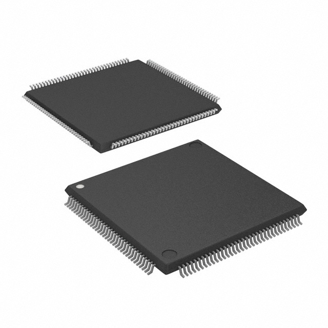
A54SX32-BG329
| Part Description |
SX Field Programmable Gate Array (FPGA) IC 249 329-BBGA |
|---|---|
| Quantity | 119 Available (as of June 14, 2026) |

| Product Category | Field Programmable Gate Array (FPGA) |
|---|---|
| Manufacturer | Microchip Technology |
| Manufacturing Status | Active |
| Manufacturer Standard Lead Time | 20 Weeks |
| Datasheet |
Specifications & Environmental
| Device Package | 329-PBGA (31x31) | Grade | Commercial | Operating Temperature | 0°C – 70°C | ||
|---|---|---|---|---|---|---|---|
| Package / Case | 329-BBGA | Number of I/O | 249 | Voltage | 3 V - 5.25 V | ||
| Mounting Method | Surface Mount | RoHS Compliance | RoHS non-compliant | REACH Compliance | REACH Unaffected | ||
| Moisture Sensitivity Level | 3 (168 Hours) | Number of LABs/CLBs | 2880 | Number of Logic Elements/Cells | 2880 | ||
| Number of Gates | 48000 | ECCN | 3A991D | HTS Code | 8542.39.0001 | ||
| Qualification | N/A |
Overview of A54SX32-BG329 – SX Field Programmable Gate Array (FPGA) IC 249 329-BBGA
The A54SX32-BG329 is a commercial-grade SX family FPGA from Microchip Technology. It provides a nonvolatile, single-chip programmable logic solution with 48,000 system gates and approximately 2,880 logic elements aimed at mid-density embedded designs.
Designed for flexible I/O and mixed-voltage systems, the device supports up to 249 user I/Os, a broad 3 V to 5.25 V supply range, and deterministic timing features suitable for PCI-compliant and other mixed-voltage applications within a 0 °C to 70 °C operating range.
Key Features
- Core Performance — Family-level performance indicators include up to 250 MHz system performance and up to 350 MHz internal performance for timing-critical logic.
- Logic Capacity — 48,000 system gates and approximately 2,880 logic elements provide mid-density programmable logic for glue logic, protocol bridging, and control functions.
- I/O and Clock Resources — Up to 249 user I/Os and 3 global clocks enable complex interfacing and synchronous designs; configurable I/O support includes 3.3 V/5 V PCI, 5 V TTL, 3.3 V LVTTL and 2.5 V LVCMOS2 signaling.
- Nonvolatile Configuration — Single-chip, nonvolatile architecture removes the need for external configuration memory and supports in-system programming and diagnostics.
- Power and Voltage — Wide supply range from 3 V to 5.25 V and power-up/power-down friendly behavior with no sequencing required for supply voltages.
- Package and Mounting — 329-BBGA package case (supplier device package: 329-PBGA, 31×31) in a surface-mount form factor suitable for compact board layouts.
- System and Test — Boundary-scan testing compliant with IEEE 1149.1 (JTAG) and in-system diagnostic capability via Silicon Explorer II for verification and debug.
- Security and Reliability — Actel Secure Programming Technology with FuseLock™ helps protect design IP against reverse engineering and unauthorized access.
- Compliance — RoHS compliant.
Typical Applications
- PCI and Mixed-Voltage Interfaces — Use the A54SX32-BG329 in PCI-compliant peripherals or bridge logic where 3.3 V/5 V PCI signaling and mixed-voltage I/O are required.
- Embedded Control and Glue Logic — Mid-density logic capacity and abundant I/Os make the device suitable for control tasks, protocol translation, and board-level glue logic.
- In-System Diagnostics and Verification — The device’s in-system diagnostic features enable verification and silicon-level debugging during development and deployment.
Unique Advantages
- Nonvolatile, single-chip solution: Eliminates external configuration memory and simplifies board-level BOM and startup sequencing.
- Flexible mixed-voltage I/O: Configurable support for multiple logic standards (including 3.3 V/5 V PCI) reduces the need for external level-shifters in mixed-voltage systems.
- Deterministic timing and high internal performance: Up to 350 MHz internal performance and deterministic timing control help meet tight timing budgets.
- Strong on-chip security: FuseLock™ programming protects intellectual property and helps prevent reverse engineering.
- Test and debug support: JTAG boundary-scan and Silicon Explorer II diagnostic support speed validation and reduce development time.
- Commercial temperature and RoHS compliant: Rated for 0 °C to 70 °C operation and RoHS-compliant packaging for general commercial applications.
Why Choose A54SX32-BG329?
The A54SX32-BG329 balances mid-range logic capacity with flexible mixed-voltage I/O and nonvolatile configuration in a compact 329-BBGA surface-mount package. With 48,000 system gates, approximately 2,880 logic elements, and up to 249 user I/Os, it is well suited for embedded designers needing a reliable, single-chip FPGA solution for PCI and mixed-signal interfacing, glue logic, and in-system verification.
Backed by Microchip Technology’s SX family feature set—including deterministic timing, in-system diagnostics, and FuseLock™ security—this device provides a scalable and maintainable platform for commercial electronic designs where compactness, configurability, and robust IP protection are important.
Request a quote or submit a purchasing inquiry to get pricing and availability for the A54SX32-BG329.


Date Founded: 1989
Headquarters: Chandler, Arizona, USA
Employees: 22,000+
Revenue: $8.349 Billion
Certifications and Memberships: ISO9001:2015, IATF16949:2016, AS 9100D


